Microsoft ends support for Internet Explorer on June 16, 2022.
We recommend using one of the browsers listed below.
- Microsoft Edge(Latest version)
- Mozilla Firefox(Latest version)
- Google Chrome(Latest version)
- Apple Safari(Latest version)
Please contact your browser provider for download and installation instructions.


July 18, 2017
High-performance optical modulators on silicon platform - Integration of compound semiconductors and silicon, providing compactness, low-power consumption, and low propagation loss -
Nippon Telegraph and Telephone Corporation (NTT; Head Office: Chiyoda-ku, Tokyo; President and CEO: Hiroo Unoura) has developed compact, low-power-consumption, and low-insertion- loss optical modulators based on silicon photonics*1 --a device-manufacturing platform for future optical communications systems. The modulators feature heterogeneous integration of indium phosphide (InP)*2 -based compound semiconductors and silicon. A device with a phase-shifter length of 0.25 millimeters exhibits 1-dB insertion loss*3 and about ten times larger modulation efficiency than conventional silicon modulators. The practical modulation speed of 32-Gbit/s was also demonstrated.
The good compatibility between the developed technology and silicon photonics means that low-cost and low-power-consumption optical circuits, including modulators and filters, will become available to handle increasing data traffic at any transmission distance in the future.
This results were announced online in "Nature Photonics" on July 17, 2017.
1.Background
Data traffic is expected to continue increasing over a wide range of transmission distances from inter-datacenters to core network systems. One of the driving forces contributing to the increase in network traffic will be the introduction of "5G"--the fifth-generation mobile network system. Mobile network traffic in 2020s is expected to be 1000 times larger than it was in 2010 [1]. It is essential to build large-capacity optical backbone network systems to support this increasing traffic, and, for this purpose compact, high-speed, and low-power-consumption optical devices are indispensable. In addition, low-cost mass-production technologies are crucial because a large number of devices are required. Silicon-based large-scale integration is the foundation of electric circuits like microprocessors*4, while InP-based compound semiconductors are now commonly used in photonic active devices for optical communications. However, InP-based devices are not suitable for mass production because of the small wafer size compared to silicon. Silicon-based optical-device manufacturing is therefore promising for sustainable development of optical communications technologies.
Mach-Zehnder optical modulators*5 (MZMs) are key devices for transmitters. They modulate continuous laser light to convert electrical signals to optical ones. The applied voltage in phase-shifter regions controls the refractive index in those regions to generate optical signals. The modulation efficiency, defined as the product of the half-wavelength voltage*6 and the phase shifter length, is the fundamental characteristic for evaluating the performance of an optical modulator. In addition, insertion loss is critical with regards to power consumption because large insertion loss requires high laser power. LiNbO3 (lithium niobate), compound semiconductors, and silicon have been applied to MZMs. Silicon has a bigger trade-off between modulation efficiency and absorption loss than the other materials do. The trade-off limits the application range of silicon photonics as the future photonic integration platform; therefore, breaking through the tradeoff is strongly required (Fig. 1).
2.Results
To break through the limitation of silicon photonics, NTT developed carrier-accumulation*7 MZMs by heterogeneously integrating InP-based compound semiconductors with silicon (Fig. 2). Carrier-accumulation modulators*8 provide higher modulation efficiency than the more common silicon-based carrier-depletion ones. Previously reported carrier-accumulation MZMs employed silicon and polysilicon. However, the optical loss caused by the increasing carrier densities and optical absorption in the polysilicon layer makes it difficult to break through the limitation of silicon-based modulators. To achieve high efficiency and low optical loss while maintaining high compatibility with silicon photonics technologies, NTT used an n-type InGaAsP membrane layer, which provides both higher modulation efficiency and lower optical loss than a polysilicon layer. The modulation efficiency of the fabricated modulators is 0.09 Vcm, which is ten times larger than that of carrier-depletion MZMs. The insertion loss of a device with a modulation length of 0.25 millimeters is 1 dB (transmittance of about 80%). These results exceed the previous limitations of silicon-based MZMs. The modulator also operates at the modulation speed of 32 Gbit/s, indicating the feasibility of using it for practical applications like 100-gigabit Ethernet*9 (Fig. 3).
3.Future developments
Large-scale integration of optical modulators and filters, making use of the features of silicon photonics technology, will provide optical transmitters with transmission capacity of over one terabit*10 per port. In addition, low-power-consumption transmitters will reduce the power consumed by intra-datacenter networks in the future.
4.Technical features
(1)Materials for phase-shifter regions: n-type InGaAsP
Electrons and holes (carriers) are used to control the refractive index of semiconductors. N-type InGaAsP provides a high-efficiency carrier-induced refractive index change because of its small effective mass compared to n-type silicon. In addition, the bandgaps*11 of InP-based compound semiconductors can be flexibly controlled by changing the composition of In, Ga, As, and P. Proper bandgap design provides both a large refractive index change and small optical loss.
(2)Device design: reducing optical loss by optimizing InGaAsP-silicon membrane layer thickness and introducing tapered structures (Fig. 4)
To improve modulation efficiency, it is essential to design the cross section so that the overlap between the area where the refractive index changes and the optical field is maximized. The refractive index change is largest at the MOS interface due to carrier accumulation; therefore, minimizing the layer thickness while maintaining strong optical confinement is essential. However, a thin layer has the drawback of large resistance, which limits modulation speed. The layer thicknesses of Si and InGaAsP were optimized to 110 and 100 nm, respectively. Taking advantage of the silicon platform, NTT introduced silicon-waveguides and tapered structures with small optical losses and reflections for input and output ports to the phase shifters. The propagation modes can be converted smoothly between the silicon wire waveguides and MOS phase shifters via 80 micrometer-long two-stage tapers.
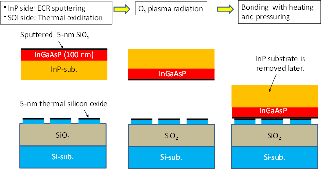
(3)Fabrication: InGaAsP-MOS interface and heterogeneous integration (Fig. 5)
Fabricating MOS structures with both InP-based semiconductors and silicon has been a challenge. Good InGaAsP-silicon MOS interfaces were obtained by using electron cyclotron resonance (ECR) sputtering to form flat insulating (SiO2) layers, followed by O2-plasma-assisted direct wafer bonding process.
Fig. 1: Modulation efficiency and insertion loss of Mach-Zehnder modulators (MZMs)
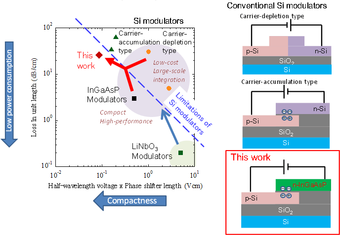
Fig. 2: Fabricated device
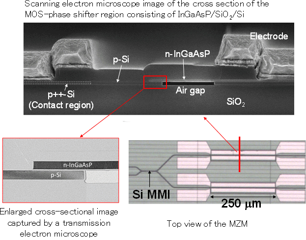
Fig. 3: High-speed modulation
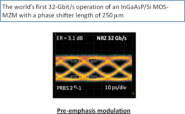
Fig. 4: Optimization of heterogeneously integrated waveguide with spot-size converters consisting of tapered waveguides
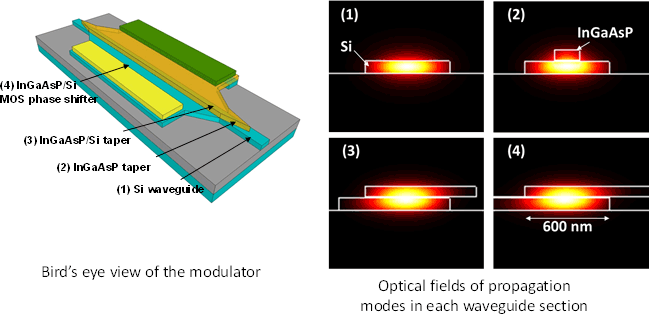
Fig. 5: Fabrication of a MOS structure with O2-plasma-assisted bonding
Glossary
*1Silicon photonics technology
An optical circuit fabrication technology using the fabrication process for silicon-based large-scale integration (LSI). Optical circuits with a waveguide width of several hundred nanometers are available. The technology is considered to be the foundation of large-scale photonic integrated circuits because large-scale silicon wafers can be employed.
*2InP-based compound semiconductors
InP is a group III-V compound semiconductor consisting of indium (In) and phosphorus (P). The bandgap can be controlled by blending it with other III- and V-group materials such as gallium (Ga) and arsenic (As). InP-based compound semiconductors are used for optical devices like lasers, modulators, and detectors for optical fiber communications systems because of the consistency between the bandgap and required operating wavelength. High-speed electric circuits are also available.
*3Insertion loss
Total optical loss between an input and output port of a modulator.
*4Microprocessor
Integrated semiconductor chips with computing functions, commonly consisting of silicon CMOS circuits*13.
*5Mach-Zehnder modulator (MZM)
Modulators consisting of two waveguides including phase-shifter regions and couplers. Electric signals applied to the phase shifters change the refractive index to generate modulated signals. The refractive index change controls the interference between two bifurcated lightwaves. MZMs can generate both intensity- and phase-modulated signals. They have been used in large-capacity transmission systems to generate multilevel-modulation signals.
*6Half-wavelength voltage
A voltage applied to an MZM to change the output light intensity from minimum to maximum. The voltage is used to evaluate the performance of MZMs. It is called as a half-wavelength voltage because the phase change in the modulators corresponds to half of the operating wavelength during the voltage change.
*7Carrier-accumulation modulator
Electrons and holes are called carriers: mediums for electron charge in semiconductors. The MOS structure*12, a fundamental structure for LSI circuits, is used for carrier-accumulation modulators. The refractive index is controlled by accumulating carriers around the MOS interface via forward bias voltage.
*8Carrier-depletion modulator
Carrier-depletion optical modulators employ pn-junction structures. The refractive index is controlled by the depletion of carriers around the pn-junction interface via reverse bias voltage.
*9100-gigabit Ethernet
The standard for transmission systems (Ethernet) to transmit 100 gigabits of data per second. For example, one of the standards employs four transmitters, each capable of 25-Gbit/s transmission. These transmitters are widely employed in datacenters and super computers.
*101 terabit
One trillion bits: ten times more data than 100 gigabits. More than one-terabit data transmission will likely be required in the future because of increasing data traffic.
*11Bandgap
The energy range where electrons cannot exist in the energy band structure in a crystal. A crystal cannot absorb light with a wavelength larger than the bandgap wavelength.
*12MOS structure
A layer structure consisting of metal, oxide, and semiconductor. The basic element for silicon CMOS (Complementary Metal Oxide Semiconductor)*13 used in microprocessors. The interface between the oxide and semiconductor is called the MOS interface.
*13Silicon CMOS transistor
The basic transistor elements in large scale integrated circuit, especially used for large scale integrated circuits with low-power consumption.
Contact information
Nippon Telegraph and Telephone Corporation
NTT Science and Core Technology Laboratory Group
Public Relations: a-info@lab.ntt.co.jp

Information is current as of the date of issue of the individual press release.
Please be advised that information may be outdated after that point.


NTT STORY
WEB media that thinks about the future with NTT