Microsoft ends support for Internet Explorer on June 16, 2022.
We recommend using one of the browsers listed below.
- Microsoft Edge(Latest version)
- Mozilla Firefox(Latest version)
- Google Chrome(Latest version)
- Apple Safari(Latest version)
Please contact your browser provider for download and installation instructions.


July 22, 2024
NTT Corporation
Electrical generation, propagation control, and detection of the ultrashort graphene plasmon wave packets
Contributing to the realization of ultrahigh-speed signal processing at terahertz frequency
(This press release was published in Japanese on July 22, 2024.)
News Highlights:
- We succeeded in transmitting the shortest graphene plasmon wave packet (pulse width of 1.2 picoseconds (picosecond =1/1 trillion second)) on a chip
- We have succeeded in modulating the phase and amplitude of terahertz electrical signals by controlling plasmons
- This achievement demonstrates a new method for controlling terahertz electrical signals on a circuit and is expected to contribute to realizing ultrahigh-speed signal processing
TOKYO - July 22, 2024 - NTT Corporation (Headquarters: Chiyoda Ward, Tokyo; Representative Member of the Board and President: Akira Shimada; hereinafter "NTT") has succeeded in electrically generating and controlling the propagation of graphene plasmon1 wave packets2 with the shortest pulse width of 1.2 picoseconds. This result shows that the phase and amplitude of a terahertz signal can be controlled electrically by using graphene plasmon. It enables terahertz signal processing a method different from conventional electrical circuit technology using transistors and is expected to contribute to realizing ultrahigh-speed signal processing in the future.
This research was conducted with The University of Tokyo and the National Institute for Materials Science (NIMS). It was published in the British science journal Nature Electronics on July 17, 2024.
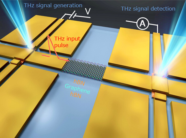 Figure 1 Diagram of the Experiment
Note. A THz electrical input pulse with a pulse width of 1.2 picoseconds was applied to graphene on a chip to generate and propagate a graphene plasmon wave packet, and its real-time waveform was measured with sub-picosecond temporal resolution. (hBN: hexagonal boron nitride)
1. Background
The terahertz (THz) region3, located between light and radio waves, has long been considered an unexplored area. However, with the rapid development of generation and detection technologies in recent years, high-speed wireless communication, sensing, and imaging using THz waves propagating in free space are gradually finding their way to social implementation. On the other hand, control technology for THz electrical signals in circuits is still under development, and in general, the signal band that an integrated circuit can handle is limited in the gigahertz (GHz) band. This indicates that there is a limit to the simple extension of existing electronic technology, and it is essential to explore new methodologies to realize faster signal processing.
This research focused on graphene plasmon as a new control technique for THz electric signals. As graphene plasmons confine THz waves in a small region and allow for the electrical control of properties such as wavelength via external voltage, research into THz wave filter and sensor applications is actively being conducted. If these characteristics can be utilized to manage THz electric signals in circuits, it will be possible to develop new ultra-high-speed electronics technologies. Initially, it was unclear whether it was possible to generate and control graphene plasmons electrically in the THz region.
2. Result of the research
The research group evaluated the propagation characteristics and controllability of graphene plasmon wave packets and the plasmon generation efficiency by injecting ultrashort input pulses (3. Key points of this research (1) and Figure 2) in the THz region generated using laser pulses into a graphene device (3. Key points of this research (2) and Figure 3).
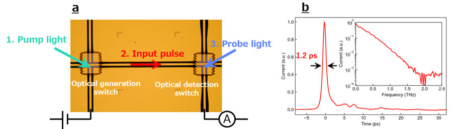 Figure 2 (a): Pump/probe spectroscopy combined with a laser pulse and a photoconductive switch enables the generation and detection of THz input pulses on a waveguide. (b): The actual measured THz input pulse. It has a pulse width of 1.2 ps and a frequency component of 0-2 THz.
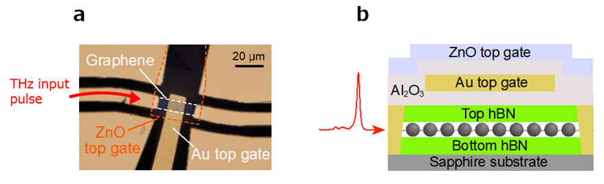 Figure 3 (a): By inserting a graphene device on the waveguide shown in Fig. 2 (a), the THz input pulse was converted into a graphene plasmon. (b): Cross-sectional diagram of a graphene device. The Au top gate controls the phase and amplitude of graphene plasmon, and the ZnO (zinc oxide) top gate increases the conversion efficiency between electrical pulse and plasmon.
As a result, the following three points became clear for the first time in this experiment.
- We succeeded in generating, controlling, and measuring 1.2 picosecond ultrashort graphene plasmon wave packets on a chip (Figure 4 (a)). This pulse width is equivalent to the time width of the input pulse before injection, and it is the shortest electrically excited plasmon wave packet in existence. This indicates that electrical signals in the THz range can be transmitted without distortion.
- We found that the phase and amplitude of the plasmon wave packet can be controlled by electrically modulating the charge density of graphene with a gate (Figure 4 (b)). Phase and amplitude control is the basic operation to realize all kinds of signal processing, which means that we have demonstrated a new device operation to handle electrical signals in the THz range.
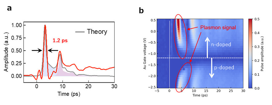 Figure 4 (a): Real-time waveforms of graphene plasmon wave packets at a metal gate voltage of 1.5 V. The peak exists after 9ps is due to multiple reflections in the circuit. (b): Gate voltage dependence of plasmon wave packet. The amplitude of the plasmon signal varies with the voltage. Further, the propagation time of the signal increases as it approaches the charge neutral point, indicating that the phase changes with the voltage.
- By optimizing the gate electrode material, we reached a maximum conversion efficiency of 35% from input pulses to graphene plasmon wave packets (Figure 5). This value exceeds the conventional light-to-plasmon conversion efficiency4 by several orders of magnitude, making graphene plasmons inherently suitable for handling electrical signals in the THz region. Furthermore, we clarified that not only the conversion efficiency but also the confinement effect, propagation velocity, and pulse width are significantly influenced by the gate electrode. These findings make it possible to optimize the device structure according to the intended purpose.
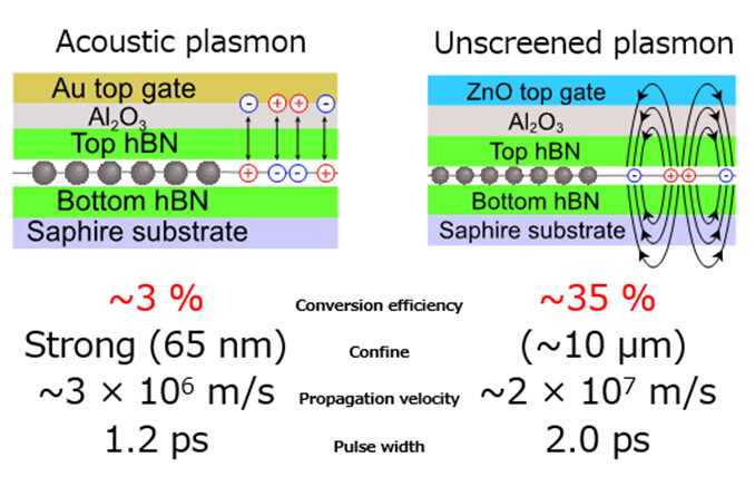 Figure 5 Diagram of different devices and comparison of the properties of each plasmon wave packet. Four features vary greatly depending on the gate electrode material.
In this research, we used the highest quality hexagonal boron nitride (hBN) grown by NIMS to fabricate and measure a clean device that protects both sides of graphene at NTT in cooperation with The University of Tokyo.
3. Key points of this research
(1) Generation and detection of ultrashort input pulses using THz electronics technology
It is still difficult to generate and detect electrical pulses in the THz region using existing electronics technology. We applied on-chip THz spectroscopy, which combines femtosecond (1/1000 trillion second) optical pulses with a photoconductive switch, to enable the generation and detection of electrical signals in a bandwidth of up to 2 THz.
(2) Graphene device
The use of Au gate enabled the generation of graphene plasmons with a large confinement effect. Furthermore, by adding a zinc oxide (ZnO) gate transparent to the THz signal, high-efficiency plasmon excitation became possible.
In this research, by integrating the technologies (1) and (2) on the same device for the first time, we succeeded in electrical generation, propagation control, and detection of ultrashort graphene plasmon wave packets, and enabled us to understand their characteristics in detail.
4. Outlook
These results show that a plasmonic device capable of electrically controlling the phase and amplitude of THz electrical signals in circuits can be implemented. By developing this technology, we aim to realize more advanced signal processing elements such as variable frequency filters, amplifiers, and modulators in the THz region. This research shows that graphene plasmons can be handled with electricity, but considering that plasmons can also be generated by light, it may lead to the development of new photonics-electric convergence technologies.
We expect that further development of signal processing technology in the THz region will contribute to significant improvements in information and communications, as well as computational processing speed in the future.
Research paper information
Journal Name: Nature Electronics
Title: On-chip transfer of ultrashort graphene plasmon wave packets using terahertz electronics
Authors: Katsuasa Yoshioka, Guillaume Bernard, Taro Wakamura, Masayuki Hashisaka, Ken-ichi Sasaki, Satoshi Sasaki, Kenji Watanabe, Takashi Taniguchi, and Norio Kumada
DOI:https://doi.org/10.1038/s41928-024-01197-x![]()
1Graphene plasmon
Plasmon is an oscillation of the electric charge density. It has the characteristics of a wave-like light, but the electromagnetic field can be confined in an extremely small area compared to light in free space. Graphene plasmons, which are oscillations of free electrons in graphene, are known to have a small loss in the THz region. They are characterized by the ability to control the wavelength, propagation speed, and other properties by changing the electron density. The shortest pulse width of the electrically generated graphene plasmon wave packet was around 25 ps (NTT survey: Phys. Rev. Lett. 110, 016801 (2013)). We reached the THz region for the first time. For further details on graphene plasmons, see Appendix.
![]() Appendix
Appendix
2Wave packet
In this study, an ultrashort input pulse with a wide frequency component of 0 to 2 THz is used, so a plasmon wave packet, which is a synthesis of many waves with different wavenumbers, is generated. A wave packet is a wave that exists only in a limited area and behaves like a moving mass of waves. The relation between the pulse width of the wave packet and the frequency component of the wave packet is connected by the Fourier transform. In this study, the propagation measurement of the wave packet which is advantageous for the proof of principle was carried out. The amplitude and phase control of the plasmon signal can be similarly demonstrated using the continuous wave with constant amplitude and frequency.
3Terahertz (THz) range
The THz region is a frequency region located between light waves and radio waves, and generally refers to electromagnetic waves of 0.1 THz to 10 THz. Electronics technology has been developed in the lower frequency region of gigahertz (GHz) (<100 GHz), while photonics technology can be used in the higher frequency range (>10 THz). However, the THz region has not yet been fully applied in industry due to difficulties of handling.
4Conversion efficiency
Graphene plasmons in the THz region have been studied by using electromagnetic fields propagating in free space (or light). In this case, it is known that the momentum mismatch between light and plasmon lowers the conversion efficiency. In particular, the conversion efficiency to a propagating plasmon wave packet is only around 0.005% (NTT survey: Nat. Photonics 12, 22 (2018)).
About NTT
NTT contributes to a sustainable society through the power of innovation. We are a leading global technology company providing services to consumers and businesses as a mobile operator, infrastructure, networks, applications, and consulting provider. Our offerings include digital business consulting, managed application services, workplace and cloud solutions, data center and edge computing, all supported by our deep global industry expertise. We are over $97B in revenue and 330,000 employees, with $3.6B in annual R&D investments. Our operations span across 80+ countries and regions, allowing us to serve clients in over 190 of them. We serve over 75% of Fortune Global 100 companies, thousands of other enterprise and government clients and millions of consumers.
Media contact
NTT Science and Core Technology Laboratory Group
Public Relations
nttrd-pr@ml.ntt.com
Information is current as of the date of issue of the individual press release.
Please be advised that information may be outdated after that point.


NTT STORY
WEB media that thinks about the future with NTT