Microsoft ends support for Internet Explorer on June 16, 2022.
We recommend using one of the browsers listed below.
- Microsoft Edge(Latest version)
- Mozilla Firefox(Latest version)
- Google Chrome(Latest version)
- Apple Safari(Latest version)
Please contact your browser provider for download and installation instructions.
September 6, 2024
Photonic topological phase transition achieved by material phase transition
Promising for reconfigurable functional photonic integrated circuit technologies
TOKYO - September 6th, 2024 - A collaborating team of NTT Corporation (NTT) and Tokyo Institute of Technology (Prof. Masaya Notomi in Physics Department) has succeeded in achieving photonic topological phase transition by material phase transition by employing novel hybrid nanostructures consisting of a phase-change material and a semiconductor nanostructure.
The wired topological properties found in solid-state materials were awarded the Nobel Prize in 1996, and this mechanism has recently been introduced into light waves in nanostructures, leading to extensive studies to explore new degrees of freedom in photonics. These photonic topological properties are generally fixed in the fabricated structures, and therefore they cannot be changed after the nanostructures are fabricated. The present achievement by NTT and Tokyo Institute of Technology has demonstrated that it is possible to change the photonic topological phase by using material phase transition in a reconfigurable manner. This achievement paves the way for novel research fields of combining material phase transition and photonic topological phase transition, and is promising for reconfigurable functional photonic integrated circuits which may lead to novel photonic information processing technologies.
This result has been just published in Science Advances on 23rd August in 2024.
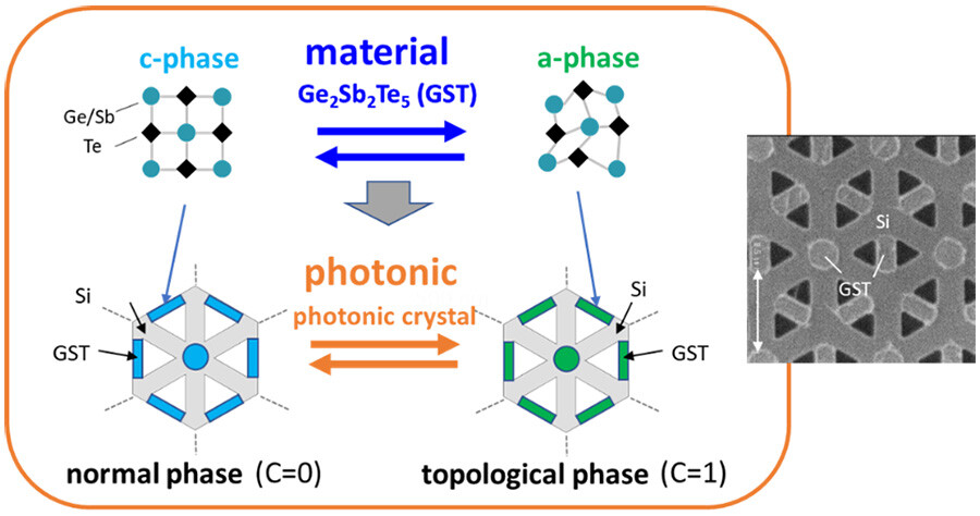 Figure 1. Summary of this work. Achievement of photonic topological phase transition induced by the material phase transition using hybrid photonic crystal structures.
1. Background
Topology is originally a concept in mathematics, and has been discussed in terms of certain discrete numbers called topological invariants1). An example of topological invariants is the genus, which is merely a number of holes in geometric structures. Such topological invariants are not changed by continuous deformation. This concept was introduced into solid-state physics some time ago, and in 1996 the Novel Prize was awarded to three physicists who found topological properties hidden in the electronic wavefunctions of solid-state materials. Their studies clarified various topological properties emerging from a topological invariant called the Chen number2), which is defined for the electronic wavefunction in solids. As one of the most notable topological properties, the topological insulator3) was found and demonstrated. Recently, similar topological properties have been found in the optical properties of photonic crystals4) which are artificial dielectric structures with periodic modulation of the refractive index, leading to the emergence of a novel research field in optics called topological photonics. When a given photonic crystal or artificial dielectric structure has non-zero Chern number, it becomes a photonic topological insulator5) in which light propagation is inhibited, but optical waveguides are automatically created at boundaries between media having different Chern numbers. These boundary waveguides have several interesting properties, such as one-way propagation and suppression of backward scattering, and they are therefore expected to be applied to future photonic integrated circuits.
In general, a phenomenon where the material properties abruptly change is called a phase transition, such as the solid-liquid or liquid-vapor phase transition. If one achieves a phase transition between the photonic topological insulating phase and the normal phase, one can create these boundaries of the Chen number. This means that one can create topological optical waveguides at an arbitrary place on-demand. However, the topological properties were fixed in the fabricated structures, and it was impossible to change them after the fabrication of nanostructures. As one of examples, Figure 2 shows how to create a photonic topological insulator employing a honeycomb-lattice photonic crystal. When six triangular holes are shifted inwards, it becomes a normal photonic insulator. When six triangular holes are shifted outwards, it becomes a photonic topological insulator having a non-zero Chern number. As shown in Figure 2, the positions of the p- and d-bands are reversed. It has been shown that this band inversion creates a non-zero Chern number. Therefore, the band inversion is essentially required for the topological phase transition. Previously, there have been many studies to manipulate the photonic topological properties in a variety of ways, but none of them achieved the photonic topological phase transition because of the difficulty of band inversion.
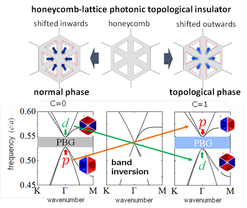 Figure 2. A way to create a honeycomb-lattice photonic topological insulator (top) and its band structure (bottom).
2. Notable points of this work
(1) Novel structure enabling photonic topological phase transition with phase-change material.
Ge2Sb2Te5 (GST)6) is one of the best-known phase-change materials, which exhibits the phase transition between the crystalline and amorphous phases (c- and a-phases) by temperature control or optical pulse irradiation. Since the refractive index of GST changes drastically at the phase transition and the switched phase is stable for a long time without any power consumption, GST has been applied to various optical devices, such as rewritable DVDs. Recently, extensive studies have been carried out on GST for optical memories and circuits. The basic idea of the present study is to load a GST film on a Si photonic crystal to exploit the large refractive index change of GST at the phase transition to induce the photonic topological phase transition in photonic crystals without changing the structure. However, it was found that it is impossible to induce the band inversion, that is, to change the Chern number, by naively loading a homogenous GST film. The team from NTT and Tokyo Tech found that it is indeed possible to induce band inversion by placing an appropriately-patterned GST film on a Si photonic crystal, as shown in Fig.3(left). With this structure, when the GST undergoes the phase transition from the crystalline phase to the amorphous phase, the photonic bands are inverted, leading to the photonic topological phase transition from the normal phase to the topological phase (Fig. 3(right)). Such a mechanism has not been reported before.
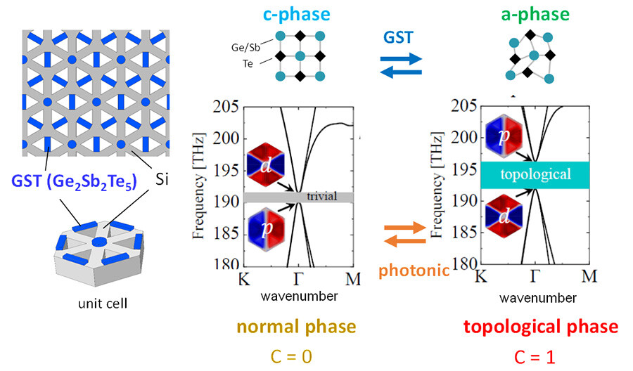 Figure 3. A schematic of the proposed hybrid photonic crystal structure (left). Calculated photonic band structures. When GST is in the c-phase (a-phase), it is in the normal (topological) phase.
(2) Accurate nanofabrication of hybrid photonic crystals.
In order to fabricate the structure proposed in Figure 3, it is necessary to fabricate different patterns for the silicon and GST layers separately. In most of previous photonic crystals consisting of multiple materials, the pattern is the same for all materials, which does not meet the requirement. The NTT-Tokyo Tech team has succeeded in accurately fabricating the proposed structure by establishing a fine two-step electron-beam lithography technology that can create an arbitrary pattern of a thin film on a semiconductor photonic crystal. This was achieved by combining ultra-fine electron-beam lithography with an accurate position alignment technique. The actual fabrication process is illustrated in Fig. 4(top). Figure 4(bottom) shows two scanning electron microscope images and one atomic force microscope image for the hybrid photonic crystal fabricated using this technology. As can be seen from these images, two different deep sub-micron patterns for the silicon and GST layers are appropriately formed, and the structure proposed in Figure 3 is successfully and accurately fabricated.
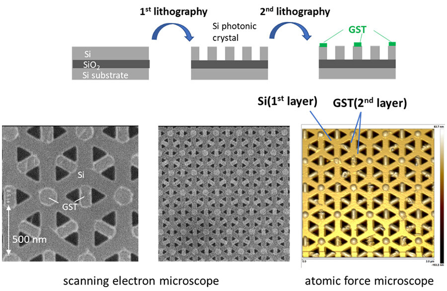 Figure 4. Schematic of the fabrication process for the hybrid photonic crystals (top). Scanning microscope images and an atomic force microscope image for the fabricated sample (bottom).
3. Experimental results
Figure 5 shows the measured photonic band structure for the fabricated hybrid photonic crystal. The photonic band measurement was performed using the angle-resolved reflection spectroscopy7). The data on the left was taken for the hybrid photonic crystal when GST is in the crystalline phase, and the data on the right was taken when GST is in the amorphous phase. Note that both data were taken for the identical sample. Two parabolic curves with opposite directions correspond to the photonic bands. An important point is that the bottom of the upper band is brighter in the left data, but the top of the lower band is brighter in the right data. This inversion of the brightness proves that the band inversion between two bands, that is, the topological phase transition, occurs during the GST phase transition. More detailed experiments show that when GST is in the crystalline phase, this photonic crystal is in the normal phase with the Chern number is 0, and when GST is in the amorphous phase, it is in the topological phase with the Chern number is 1. These experimental results have clarified that the photonic topological phase transition takes place as a result of the material phase transition of GST.
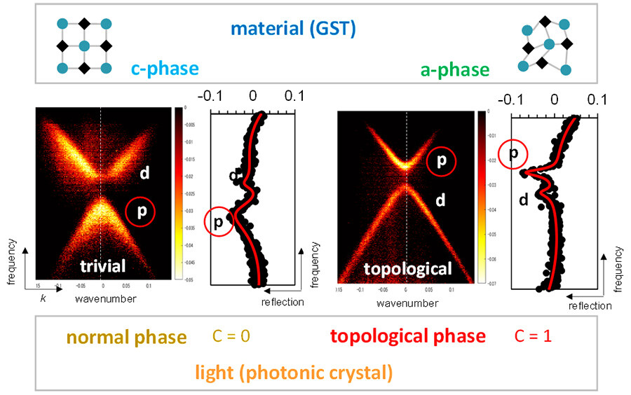 Figure 5. Photonic band structures measured by the angle-resolved reflection spectroscopy. As a result of the material phase transition of GST, the brightness of two bands is reversed, showing that the photonic topological phase transition takes place.
This is the first demonstration of the photonic topological phase transition caused by the material phase transition. This work also succeeds in linking two fundamentally different phase transitions in a unique way, which may pave the way for novel research directions. Furthermore, the present result indicates that one can set a photonic crystal in the normal or topological phase arbitrarily. Since the material phase of GST can be altered in both directions by optical or electric pulse excitation, one can change the photonic phase of an arbitrary region of the prefabricated photonic crystal by such local excitations, which means that one can create topological boundary waveguides with different Chern numbers at any place in the circuit in a reconfigurable manner. Thus, the present result is an important step towards reconfigurable photonic topological circuit technologies, as illustrated in Figure 6.
4. Outlook
The NTT-Tokyo Tech team is planning to extend the present study to the optical pulse control of topological boundary waveguides, and aiming at applications in reconfigurable photonic topological circuits. They are also interested in pursuing this controllability of the photonic topological phase as a novel degree of freedom in photonic information processing. Topological photonics is currently an active field of fundamental research where novel phenomena are being discovered one after the other. The present result may offer a way to control such a new aspect of topological photonics, and thus may have a wide applicability in terms of fundamental and applied research.
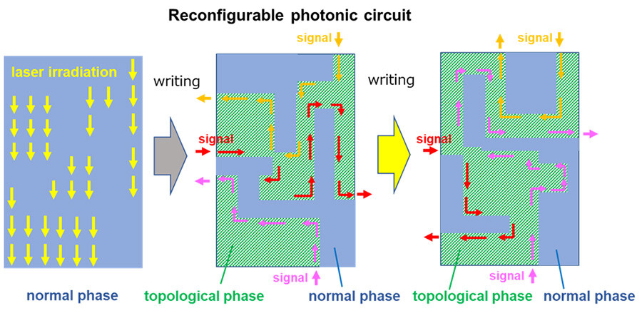 Figure 6. A conceptional image for reconfigurable photonic circuits using the photonic topological phase transition induced by the GST phase transition controlled by the laser irradiation.
Journal information
"Photonic topological phase transition induced by material phase transition", Takahiro Uemura, Yuto Moritake, Taiki Yoda, Hisashi Chiba, Yusuke Tanaka, Masaaki Ono, Eiichi Kuramochi, and Masaya Notomi,
Science Advances 10, eadp7779 (2024)
DOI: 10.1126/sciadv.adp7779
1Topological invariant: A discrete number (integer or half-integer) representing topological properties, which does not change by continuous deformation.
2Chern number: One of topological invariants defined for waves in periodic structures. When Chern number becomes non-zero, topological properties show up.
3Topological insulator: It is an insulator as a bulk, but it has propagating states at the surface or boundary with different Chern numbers. These propagating states have several interesting properties, such as one-way propagation fixed by the orientation of spins.
4Photonic crystal: An artificial dielectric structure with a periodic refractive-index modulation in a light wavelength scale, which is generally fabricated by modern nanofabrication technologies.
5Photonic topological insulator: An optical analog of a topological insulator, which have a non-zero Chen number. It is a photonic insulator as a bulk, but an optical waveguide can be created at a boundary between photonic crystals having different Chern numbers.
6GST (Ge2Sb2Te5): A chalcogenide phase-change material which has two stable states (crystalline and amorphous phases) at room temperature. The phase transition between two phases can be caused by temporal temperature change or current/light pulse injection. Since the refractive indices for two phases are largely different, GST has been applied for various optical memory devices.
7Angle-resolved reflection spectroscopy: A method for measuring the photonic band structure of photonic crystals, where one employs angle-resolved reflection at the surface of photonic crystals.
About NTT
NTT contributes to a sustainable society through the power of innovation. We are a leading global technology company providing services to consumers and business as a mobile operator, infrastructure, networks, applications, and consulting provider. Our offerings include digital business consulting, managed application services, workplace and cloud solutions, data center and edge computing, all supported by our deep global industry expertise. We are over $97B in revenue and 330,000 employees, with $3.6B in annual R&D investments. Our operations span across 80+ countries and regions, allowing us to serve clients in over 190 of them. We serve over 75% of Fortune Global 100 companies, thousands of other enterprise and government clients and millions of consumers.
About Tokyo Institute of Technology
Tokyo Tech stands at the forefront of research and higher education as the leading university for science and technology in Japan. Tokyo Tech researchers excel in fields ranging from materials science to biology, computer science, and physics. Founded in 1881, Tokyo Tech hosts over 10,000 undergraduate and graduate students per year, who develop into scientific leaders and some of the most sought-after engineers in industry. Embodying the Japanese philosophy of "monotsukuri," meaning "technical ingenuity and innovation," the Tokyo Tech community strives to contribute to society through high-impact research.
https://www.titech.ac.jp/english/
Institute of Science Tokyo (Science Tokyo) will be established on October 1, 2024, following the merger between Tokyo Medical and Dental University (TMDU) and Tokyo Institute of Technology (Tokyo Tech), with the mission of "Advancing science and human wellbeing to create value for and with society."
https://www.isct.ac.jp/en
Media contact
NTT Science and Core Technology Laboratory Group
nttrd-pr@ml.ntt.com
Tokyo Institute of Technology
media@jim,titech.ac.jp
Information is current as of the date of issue of the individual press release.
Please be advised that information may be outdated after that point.
NTT STORY
WEB media that thinks about the future with NTT


