Microsoft ends support for Internet Explorer on June 16, 2022.
We recommend using one of the browsers listed below.
- Microsoft Edge(Latest version)
- Mozilla Firefox(Latest version)
- Google Chrome(Latest version)
- Apple Safari(Latest version)
Please contact your browser provider for download and installation instructions.
October 28, 2024
NTT Corporation
Compact wireless device which enables sub-terahertz ultra high-speed wireless communication in 6G
World's highest data transmission rate of 160Gbps in the 300GHz band by using InP integrated IC technology
News Highlights:
- In the 300 GHz band, which is expected to be applied to future applications of wireless communications, we have realized a compact wireless front-end (FE)1 using the InP-HEMT2, a high-speed transistor and our proprietary high-frequency analog circuit design technology
- Achieved the world's highest data transmission rate of 160Gbps at FE using 300 GHz band semiconductor electronic circuits
- Expected to be used for ultra-high-speed wireless communications supporting various use cases proposed in the 6G mobile communication system
TOKYO - October 28, 2024 - NTT Corporation (Headquarters: Chiyoda Ward, Tokyo; Representative Member of the Board and President: Akira Shimada; hereinafter "NTT") has developed a compact wireless FE, which is hardware for wireless communications in the 300 GHz band expected to be applied to ultra high-speed wireless communications. To reduce the size of the FE and increase the bandwidth (improve the data rate), we challenged the one-chip integration of the component circuits constituting the FE and proposed an FE circuit configuration to eliminate the problem of local oscillator (LO) leakage3. This FE circuit was fabricated using NTT's in-house semiconductor technology, InP-HEMT to realize a compact wireless FE with a significantly wider operating bandwidth compared to conventional FEs [1]. We conducted data transmission experiments using a compact wireless FE and achieved the world's highest data rate of 160Gbps in the 300 GHz band.
The results of this research will be presented at an international conference "IEEE BiCMOS and Compound Semiconductor Integrated Circuits and Technology Symposium 2024" on October 28, 2024.
Research background
In 6G [2], various use cases have been proposed, such as immersive communication, telemedicine, and autonomous driving. To realize ultra-high speed wireless communication exceeding 100Gbps, which is required to support such use cases, communication applications in the sub-terahertz band (frequency band between 100 GHz and 300 GHz), which has a wide bandwidth available, are expected to be realized. For communication applications, it is necessary to realize wireless FE, which is hardware with functions (such as amplification and frequency conversion) necessary for transmitting and receiving radio waves in the sub-terahertz band. NTT has been engaged in the research and development of an FE capable of ultra-high-speed wireless communication in the 300 GHz band. By integrating FE components, we have realized a compact FE capable of ultra-high-speed communication and achieved the world's highest data rate of 160 Gbps in the 300 GHz band (Figure 1).
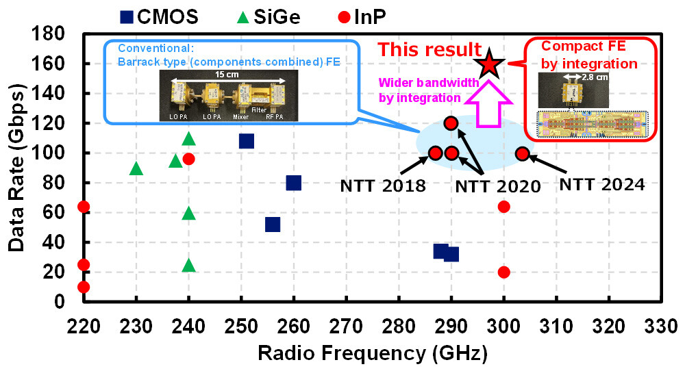 Figure 1 Positioning of this Work
Note. Radio Frequency (RF) refers to the center frequency of the band used for radio communication. CMOS, SiGe, and InP in the legend refer to the technology used in FE. CMOS (Complementary Metal-Oxide Semiconductor) is a field effect transistor technology using semiconductor silicon (Si), and SiGe is a bipolar transistor technology using semiconductor silicon germanium.
Research content
The FE has a Transmitter (TX) that transmits radio signals and a Receiver (RX) that receives radio signals (Figure 2). The FE consists of an analog circuit that converts the data signal generated by the baseband/IF section into a 300 GHz band RF signal. The TX consists of a mixer for frequency conversion, an RF power amplifier (RF PA) to amplify the RF signal generated by the mixer, and an LO power amplifier (LO PA) to secure the LO signal power required to drive the mixer. The RX consists of a mixer, a low noise amplifier (LNA) to amplify the received RF signal to low noise, and an LO PA. These components must operate in the 300 GHz band to achieve FE in the 300 GHz band.
 Figure 2 FE Configuration
Note. The IF (intermediate frequency) signal is a lower frequency signal than the RF signal used in FE. The LO (local oscillator) signal drives a mixer that converts frequencies between IF and RF signals.
NTT has been engaged in the research and development of 300 GHz band FEs using InP-HEMT technology, a high-speed transistor developed over many years, and high-frequency analog circuit design technology. In 2020, we achieved the world's highest data rate of 120Gbps using the FE we manufactured [1].
Conventional FEs have been designed and manufactured as individual modules, including amplifiers and mixers that perform frequency conversion and implemented in a form that combines them (barrack type). However, while it is possible to create a flexible FE configuration by freely combining components, there are two issues:
- Since multiple modules are combined to build an FE, the size of the FE becomes large
- Multiple connections between modules (causing loss or bandwidth reduction) limit FE operating bandwidth, making it difficult to improve data rates
To solve these problems, we have been working on integrating FE components into a single integrated circuit (IC). If FE can be realized with one module by integration, (1) can be solved, and (2) can also be solved by eliminating connections between modules.
LO leakage, which is an unnecessary wave generated in the mixer, is a major issue in integrating FE. LO leakages should be eliminated because they adversely affect the operation of other circuits integrated with the mixer and degrade the quality of the signal transmitted by the FE. In the barrack configuration, this problem can be solved by providing a filter capable of eliminating the LO leakage, but it is difficult to eliminate the LO leakage within a single integrated circuit in the sub-terahertz band. For this reason, we have studied a differential configuration4 FE that can eliminate LO leakage inside the integrated circuit even in the sub-terahertz band (Figure 3).
In the TX, the mixer, LO power amplifier (LO PA) for driving the mixer, and RF power amplifier (RF PA) for amplifying the 300 GHz band signal (RF signal) generated by the mixer are integrated as component circuits. All these component circuits have a differential configuration.
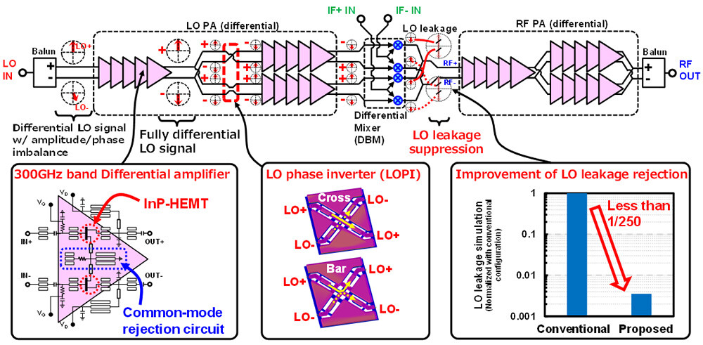 Figure 3 Circuit Configuration of Proposed 300 GHz Band FE (TX)
In the FE of the differential configuration, the LO leakage is eliminated by interfering the LO leakage in the opposite phase in the post-mixer stage. This requires the mixer to be driven by a fully differential LO signal (two LO signals of equal amplitude and 180° different phase.) To generate a fully differential LO signal, a differential amplifier is required in addition to the differential signal generator balun5. Differential amplifiers are required to compensate for amplitude errors and phase deviations from 180° in differential signals output from baluns (common mode rejection function)6. By applying NTT's proprietary common mode rejection function circuit [3] to each amplification stage of the LO PA, we succeeded in generating a fully differential LO signal by the LO PA. In addition, by combining the LO phase inverter circuit (LOPI), the LO leakage is eliminated in the post-mixer stage. As a result of these efforts, the LO leakage was significantly reduced to less than 1/250 compared to the conventional configuration (single-end configuration), and the FE was successfully integrated into a single chip (Figure 4). The FE is mounted on a metal package using a unique mounting technology using a 300 GHz band waveguide coupler (ridge coupler) and is modularized. As a result of one-chip integration, the FE has been significantly reduced from 15 cm to 2.8 cm (Figure 5).
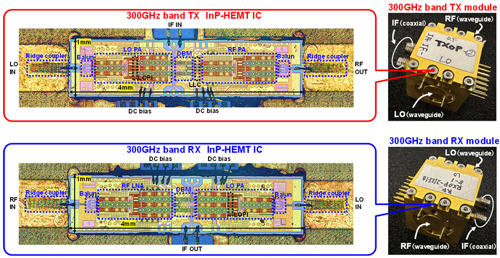 Figure 4 300 GHz band TX and RX ICs and Modules Fabricated Using NTT's In-house InP-HEMT Technology
 Figure 5 Smaller Module Size by Integrating Components
In addition, from the frequency characteristics of the conversion gain7 of the FE, the operating bandwidth has been greatly improved compared to the conventional FE [1] by eliminating the module connection due to integration (Figure 6). To evaluate the performance of the newly manufactured FE, we conducted data transmission experiments using the measurement system shown in Figure 7. A commercially available multiplier and synthesizer were used to generate the LO signal. By expanding the FE operating bandwidth, 16QAM modulated signals (multilevel modulation (number of bits that can be transmitted at one time: 4) can be transmitted with high signal quality (signal-to-noise ratio8: 16.5dB or more) using a wide bandwidth with a symbol rate of 40Gbaud. This means that 160Gbps transmission was successfully achieved in the 300 GHz band. This data rate is the highest in the world for FE in the 300 GHz band, as shown in Figure 1.
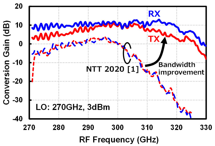 Figure 6 Improvement of Operating Bandwidth of TX and RX by One-chip Integration of Components
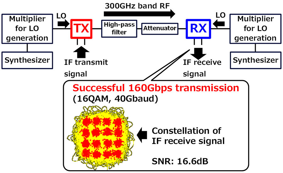 Figure 7 Data Transmission Experiment
Outlook and social significance
The newly realized FE directly connects TX and RX for data transmission. By connecting antennas to TX and RX and conducting performance evaluation in an actual wireless environment, we will demonstrate the effectiveness of the sub-terahertz band for realizing future ultra-high-speed wireless communications. We will also integrate functions such as the LO signal generator and IF amplifier into FE to further improve quality. Through these R&D efforts, we aim to realize ultra-high-speed wireless communications that support the various use cases proposed for 6G.
International conference
Conference Name: "IEEE BiCMOS and Compound Semiconductor Integrated Circuits and Technology Symposium 2024 (BCICTS 2024)"
Location: Fort Lauderdale, USA
Date: October 27, 2024 - October 30, 2024
Title: 300 GHz 160 Gb/s InP-HEMT Wireless Front-End with Fully Differential Architecture
Authors: Hiroshi Hamada, Ibrahim Abdo, Takuya Tsutsumi, Hiroyuki Takahashi (4)
[1] H. Hamada et al., "300-GHz-Band 120-Gb/s Wireless Front-End Based on InP-HEMT PAs and Mixers," IEEE J. Solid-State Circuits, vol. 55, no. 9, pp. 2316-2335, Sep. 2020.,
https://doi.org/10.1109/JSSC.2020.3005818.
[2] DOCOMO 6G White Paper (https://www.docomo.ne.jp/corporate/technology/whitepaper_6g/)
[3] H. Hamada et al., "220–325-GHz 25-dB-Gain Differential Amplifier With High Common-Mode-Rejection Circuit in 60-nm InP-HEMT Technology," IEEE Microw. Wireless Compon. Lett., vol. 31, no. 6, pp. 709-712, Jun. 2021.,
https://doi.org/10.1109/LMWC.2021.3061662.
1Front-end (FE)
Front-end (FE) is a general term for a group of analog circuits located between an antenna that exchanges radio waves with space and a baseband unit (digital circuit) that processes data superimposed on radio waves in a transceiver, which is the hardware for wireless communication. It is so named because it is placed in the transceiver closest to the radio wave.
2InP-HEMT
HEMTs (High Electron Mobility Transistors) are a type of transistor used in electronic circuits known for their high-frequency characteristics due to their high electron mobility. HEMTs made on an indium-phosphorus (InP) semiconductor substrate are called InP-HEMTs. InP-HEMTs are semiconductors that can grow crystals on InP substrates, and because InGaAs (indium gallium arsenide), which has a very high electron mobility, can be used as the electron transport layer, they have even better high-frequency characteristics among HEMTs.
3LO leakage
The mixer converts low-frequency signals into high-frequency signals such as 300 GHz by using local oscillator (LO) signals. Part of this LO signal leakage from the mixer, is called an LO leakage. If the LO leakage is input to the amplifier, the gain of the amplifier will be reduced, and other circuits will be adversely affected.
4Differential configuration
A circuit configuration that uses the potential difference between a pair of signals (differential pair) whose phases differ by 180° as an electrical signal. Another circuit configuration that uses the potential difference between the signal and the ground potential as the signal is called a single-ended configuration. A differential circuit has advantages such as being resistant to external noise and eliminating LO leakage.
5Balun
A circuit with a function to convert between a single-ended signal and a differential signal.
6Common mode rejection function
An electrical signal of the same phase (in-phase signal) may propagate into a differential pair in which electrical signals of 180° different phases are propagated. It is desirable to eliminate the in-phase signal because it has the effect of losing the advantage of the differential configuration. Therefore, a differential amplifier with the function of selectively amplifying the differential signal and not amplifying (or attenuating) the in-phase signal is important. This function of the differential amplifier is called the common mode rejection function.
7Conversion gain
In circuits with frequency conversion functions such as mixers and FEs, the ratio of signal strength before and after conversion is called conversion gain. A performance index that corresponds to the gain (amplification factor) of a normal amplifier.
8Signal to noise ratio
In general, signals used for communication are superimposed with noise. The greater the amount of noise, the more difficult it is to read the signal accurately. Therefore, the signal to noise ratio (SNR), which is the ratio of the strength of signal to noise, is used as a quantity to express the communication quality. There is a correlation between bit error rate (BER) and SNR, and a good indicator is SNR (If 16QAM is used as in this case, 16.5dB is used) which corresponds to a BER of 1/1000.
About NTT
NTT contributes to a sustainable society through the power of innovation. We are a leading global technology company providing services to consumers and businesses as a mobile operator, infrastructure, networks, applications, and consulting provider. Our offerings include digital business consulting, managed application services, workplace and cloud solutions, data center and edge computing, all supported by our deep global industry expertise. We are over $97B in revenue and 330,000 employees, with $3.6B in annual R&D investments. Our operations span across 80+ countries and regions, allowing us to serve clients in over 190 of them. We serve over 75% of Fortune Global 100 companies, thousands of other enterprise and government clients and millions of consumers.
Media contact
NTT Science and Core Technology Laboratory Group
Public Relations
nttrd-pr@ml.ntt.com
Information is current as of the date of issue of the individual press release.
Please be advised that information may be outdated after that point.
NTT STORY
WEB media that thinks about the future with NTT


