Microsoft ends support for Internet Explorer on June 16, 2022.
We recommend using one of the browsers listed below.
- Microsoft Edge(Latest version)
- Mozilla Firefox(Latest version)
- Google Chrome(Latest version)
- Apple Safari(Latest version)
Please contact your browser provider for download and installation instructions.
March 8, 2016
Nippon Telegraph and Telephone Corporation
Tohoku University
Long-distance transport of electron spins for spin-based logic devices Enhancement of spin lifetime with application of an external electric field
Nippon Telegraph and Telephone Corporation (NTT, CEO: Hiroo Unoura, Tokyo) and Tohoku University (President: Susumu Satomi, Miyagi) have achieved the electrical transport of electron spins*1 over a long distance by using a specially designed compound semiconductor quantum well*2 in which the spin lifetime is enhanced by applying a specific gate bias voltage. This finding enables us to stably manipulate electron spins in semiconductors, and consequently will contribute to the realization of spin-based logic devices such as a spin field effect transistor*3 or a future quantum computer*4. A research paper describing these results will appear as an Advance Online Publication in Nature Communications on March 8, 2016.
This work was supported by Grants-in-Aid for Scientific Research from the Japan Society for the Promotion of Science (JSPS).
1.Background
Almost all electronics devices operate by using an electron charge controlled by electrical means. In addition to a charge, an electron has a spin as a magnetic property. A groundbreaking concept for information processing based on electron spins is proposed using electron spins in semiconductors. Quantum computing enables us to exceed the speed of conventional computing and a spin transistor reduces energy consumption.
However, electron spins have yet to be used in realistic electronics devices except as part of magnetic devices for information storage. The reason is that spin polarization in a semiconductor is easily randomized, and consequently it is difficult to transport spin polarization over a long distance. An electron spin itself is a quantum spin angular momentum*5. Electrical transport and the manipulation of spin polarization are essential technologies if electron spins are to be employed in a device. However, in actual materials, electron spins are randomized by the multiple scattering of electrons, resulting in spin depolarization in finite time. This phenomenon is called spin relaxation, and it results in spin polarization having a short transport length in a device. To realize spin functional devices, it is important to suppress spin relaxation and achieve more stable manipulation of electron spins.
2.Achievements
The research team has demonstrated long-distance spin transport by electrical means in a semiconductor quantum well, which is designed to increase spin lifetime. Furthermore, the research team has demonstrated that the spin precession speed of drifting electrons in semiconductor quantum wells can be controlled by applying an external gate voltage. These technological achievements combining spin transport and spin rotation will provide a way to manipulate spin polarization more stably in semiconductors and contribute to the realization of spin-based logic devices and computation.
3.Technical Features
(1)Material design of a semiconductor quantum well for a long spin lifetime
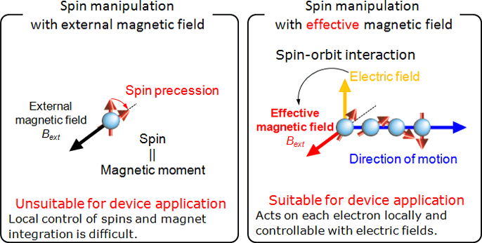
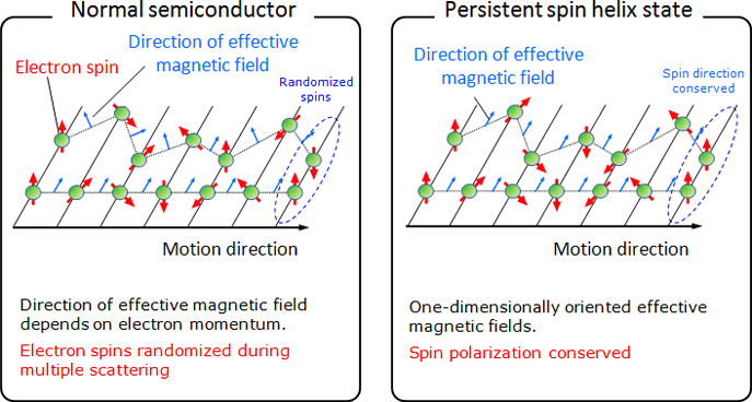
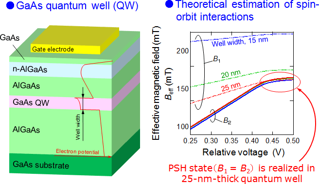
In this research, a specially designed semiconductor quantum well was used. Electron spins moving in a compound semiconductor feel the effective (not real) magnetic field induced by a spin-orbit interaction*6 (Fig. 1), and consequently precess about the effective magnetic field. Since the direction of the effective magnetic field depends on the direction of the electron momentum, the spin precession axes are randomized by the multiple scattering of electrons, and eventually the electron spins relax (Fig. 2 left panel). NTT has focused on the phenomenon whereby the direction of the effective magnetic field becomes independent of the electron momentum in the quantum well in which two spin-orbit interactions originating from different mechanisms have the same strength. Under this special condition, an electron spin can propagate in a quantum well without spin relaxation, and this is called the persistent spin helix state (Fig. 2 right panel). NTT has designed a quantum well structure to realize the persistent spin helix state based on a theoretical calculation of the spin-orbit interactions (Fig. 3), from which it is found that electron spins in a 25-nm-thick quantum well can be switched from the normal state to the persistent spin helix state by applying a gate voltage.
(2)Observation of spatial distribution of electron spins by magneto-optic Kerr effect
The spatial distributions of electron spins in quantum wells close or not close to the persistent spin helix state are measured by the magneto-optic Kerr effect*7. The sample structure we used in the experiment allowed us to apply electric fields perpendicular to the quantum well plane and in-plane electric fields along the x and y directions. As shown in Fig. 4, electron spins were transported directly over 100µm in a quantum well close to the persistent spin helix state. In addition, in this quantum well, we found that electron spins propagate with (without) spin precession in the x(y) direction, reflecting the crystal orientation dependence of effective magnetic fields in the persistent spin helix state. When we changed the strength of the spin-orbit interaction by applying a gate voltage, the spin transport length was maximized in the persistent spin helix state (Fig. 5). This experimental result indicates that spin relaxation can be suppressed in the persistent spin helix state, and spins can be transported for a longer distance than in the normal state.
4.Future Plans
The technologies demonstrated in the present research, namely the long-distance transport of electron spins and the electrical manipulation of propagating spins, will lead to the application of spins to novel spin-based logic devices, which will open door to logical operation using spins in a spin circuit. We are now planning to develop a spin-based information-processing system by incorporating elementary spin devices in a spin circuit.
Publications
Y. Kunihashi, H. Sanada, H. Gotoh, K. Onomitsu, M. Kohda, J. Nitta, and T. Sogawa
"Drift transport of helical spin coherence with tailored spin-orbit interactions"
Nature Communications (2016).
Glossary
- *1Electron spin
- An electron has the property of a small magnet. This property is called 'spin' by analogy with the rotation of a classical sphere. The spin is treated as a quantum mechanical state and represented by a vector in a three-dimensional space.
- *2Semiconductor quantum well
- A semiconductor quantum well is a layered structure of semiconductors, where a quantum well layer with a small potential energy is sandwiched between barrier layers with a larger potential energy. We can confine electrons effectively in the quantum well layer.
- *3Spin field effect transistor
- A spin field effect transistor consists of ferromagnetic source and drain electrodes and a channel consisting of a semiconductor quantum well, which produces an output signal that depends on the relative angle of magnetization between a ferromagnetic electrode and electron spins in the channel. The electric current flowing through this device is controlled by gate control of the spin directions.
- *4Quantum computer
- A quantum computer is a computer that operates with "quantum bits (qubits)" based on physical systems that are governed by quantum mechanics. The quantum computer can use the superposition of the quantum states, and can therefore solve certain problems (e.g. integer factorization, database search) much faster than a classical computer.
- *5Spin angular momentum
- Spin angular momentum is one of the degrees of freedom of an elementary particle. For an electron, spin angular momentum is quantized with a unit given by ћ/2.
- *6Spin-orbit interaction
- A spin-orbit interaction is a relativistic effect that produces an effective magnetic field for an electron moving in an electric field. The spin-orbit interaction in semiconductors is mainly induced by crystal fields and externally applied voltage.
- *7Magneto-optic Kerr effect
- The polarization of the light reflected from a magnetized material rotates slightly from the original polarization. This is called the magneto-optic Kerr effect. In the present research, the Kerr rotation angle is proportional to the spin component in the direction perpendicular to the sample plane.
Press release in Japanese
The release in Japanese was issued on March 8, 2016.
Fig. 1 Manipulation of drifting spins by using an effective magnetic field

Fig. 2 Enhancement of spin lifetime in persistent spin helix state

Fig. 3 Material design of quantum well for persistent spin helix state

Fig. 4 Spatial distribution of electron spins in persistent spin helix state
Fig. 5 Electrical manipulation of electron spins and maximized transport length with application of gate voltage
Contact:
Nippon Telegraph and Telephone Corporation
NTT Science and Core Technology Laboratory Group, PR Section
a-info@lab.ntt.co.jp
TEL: +81-46-240-5157
Tohoku University
Graduate School of Engineering, Public Relations Office
TEL: +81-22-795-5898
Information is current as of the date of issue of the individual press release.
Please be advised that information may be outdated after that point.
NTT STORY
WEB media that thinks about the future with NTT


