Microsoft ends support for Internet Explorer on June 16, 2022.
We recommend using one of the browsers listed below.
- Microsoft Edge(Latest version)
- Mozilla Firefox(Latest version)
- Google Chrome(Latest version)
- Apple Safari(Latest version)
Please contact your browser provider for download and installation instructions.


April 11, 2016
Nippon Telegraph and Telephone (NTT)
Tokyo University of Science
Attosecond time resolved electronic oscillation within gallium nitride (GaN) semiconductor --Toward petahertz semiconductor technology--
Nippon Telegraph and Telephone (NTT) Corporation (Head office, Chiyoda-ku, Tokyo, Japan; Hiroo Unoura, President and CEO) and Tokyo University of Science (Kagurazaka Campus, Shinjuku-ku, Tokyo, Japan; Akira Fujishima, University President) successfully observed electronic oscillation (dipole oscillation) with attosecond (as: 10-18 of a second) periodicity using gallium nitride (GaN) wide-bandgap semiconductor. A few-cycle near-infrared pulse induces the ultrafast electric interband polarization. The dipole oscillation with 860-as periodicity in the GaN electron and hole system is revealed by an extremely short isolated attosecond pulse. The resultant dipole frequency reaches 1.16 PHz (1015 Hz), making this the first time the petahertz frequency barrier has been exceeded with semiconductor. This study shows the potential of future petahertz signal processing technology based on ordinary wide-bandgap semiconductor devices.
This achievement is reported in Nature Physics. In addition, the study is introduced in "News and Views" of the journal on April 11, 2016.
This work was supported by JSPS KAKENHI Grant No. 25706027.
1.Background
The growing demand for unprecedented speeds and capacities in the advanced information society has been creating challenges in signal processing technology based on modern semiconductor photonics and electronics. The high-speed operation depends on ultrafast control of physical properties with radio-frequency (RF) electric fields. This principle is common to semiconductor applications ranging from the field-effect transistor, which is one of the building blocks for high-clock-rate logic operation in digital electronics, to the electro-absorption modulator for high-bit-rate transport in optical communications.
In such high-speed semiconductor devices, the current maximum operational frequency is in the terahertz (1012 Hz) regime, which is limited by the response time of band energy modulation with RF electric fields. To extend the operational frequency into the petahertz (1015 Hz) regime, lightwave field control has potential. However, to observe the ultrafast electron motion with petahertz frequency, extremely high temporal resolution is required. For example, as a camera needs a high-speed shutter to take stop-motion snap shots, an instantaneous strobe light is necessary in order to observe an electron with ultrafast motion.
2.Achievements
We demonstrate optical drive at 1.16-PHz using gallium nitride (GaN) wide-bandgap semiconductor1. A few-cycle near-infrared (NIR) pulse induces the ultrafast electric interband polarization with the multi-photon process. The dipole oscillation2 with 860-as periodicity in the GaN electron and hole system is revealed by an extremely short isolated attosecond pulse (IAP)3. The resultant dipole frequency reaches 1.16 PHz, making this the first time the petahertz frequency barrier has been exceeded with semiconductor.
Experiments
- (1)The target is epitaxially grown bulk GaN with the wurtzite structure [0001]. A few-cycle femtosecond (fs: 10-15 of a second) NIR pulse excites the electron from the valance band (VB) to the conduction band (CB) through the multi-photon process (
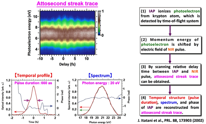
4 and produces dipole oscillation, which is monitored by the IAP with a temporal delay scan using transient absorption spectroscopy5 (Fig. 2). The measured transient absorption trace (Fig. 3) indicates the dipole oscillation with 860-as periodicity, which corresponds to 1.16 PHz (Fig. 4). - (2)The IAP is generated by using the double optical gating (DOG) technique [H. Mashiko et al., Phys. Rev. Lett. 100, 103906 (2008)] (Fig. 5). This technique combines two optical gating methods--polarization gating and two-color gating--for the driving laser:. The advantage of DOG is photon energy (frequency) tunability for IAP generation. Thus, it is useful for monitoring ultrafast phenomena in a variety of target materials. Here the IAP (20-eV center photon energy) in the vacuum ultraviolet (VUV) region is generated from argon gas, which is used for the transient absorption spectroscopy. The IAP is temporally characterized by attosecond streak method6. The pulse duration is 660 as (Fig. 6).
3.Technical Features
(1)Transient absorption spectroscopy with IAP [NTT and Tokyo University of Science]
The larger the electron transition energy is, the shorter the periodicity becomes. Since the GaN semiconductor has a wide bandgap (energy gap between the VB and CB) of 3.4 eV, the induced dipole oscillation can achieve attosecond periodicity. Transient absorption spectroscopy with the IAP is a powerful method for monitoring ultrafast electron dynamics because the absorption strongly depends on the dipole oscillation.
(2)Center photon energy tunable IAP using DOG [NTT]
In this experiment, the duration of the IAP needs to be shorter than the dipole oscillation periodicity of 860 as. In addition, its center photon energy should be reduced, because the lower photon energy is close to the VB and CB states in GaN semiconductor. However, the higher center photon energy gives shorter pulse duration. Here to satisfy both conditions, the IAP with 20-eV center photon energy in VUV region and 660-as duration is generated using the DOG technique.
4.Future Plans
The demonstrated petahertz optical drive using wide-bandgap GaN semiconductor has the potential for use in constructing high-clock-rate logic operation systems in digital photonics and electronics. In addition, this ultrafast property revealed by the direct time-domain observation will provide an ultrafast manipulation technology for dipole oscillation. The benefit is directly linked to controlling absorption, reflection, refractive indices, photocurrent, photoemission, and diffraction, which are important for implementing photonic and electronic devices with unprecedented speed in the future.
Publication information
Hiroki Mashiko, Katsuya Oguri, Tomohiko Yamaguchi, Akira Suda and Hideki Gotoh
"Petahertz optical drive with wide-bandgap semiconductor"
Nature Physics (2016)
Glossary
1.Gallium nitride (GaN) semiconductor
GaN material has wide bandgap of 3.4 eV in a wurtzite crystal structure, which is commonly used in bright light-emitting diodes. Since GaN has high breakdown voltage, high heat capacity, and high thermal conductivity, it is a promising semiconductor material for high-power and high-frequency transistors.
2.Dipole oscillation
A dipole is defined as the product of the magnitude of electric charges and the distance separating them. When an electron is excited by an incident light field, electrons and ions with opposite polarities create the dipole. Then, the dipole oscillation induces charge oscillation.
3.Attosecond pulse
An attosecond is 1×10-18 of a second. An attosecond pulse is an optical light source with ultrashort duration, which behaves as an instantaneous strobe light. Generally, the pulse exists in the VUV and XUV regions (8~90-nm wavelength, 150~15 eV photon energy). The attosecond pulse is the shortest strobe light in existence.
4.Polarization
Electric polarization is the vector field that expresses the density of permanent or induced electric dipole moments in a dielectric material. The relative shift of positive and negative electric charges in opposite directions within a dielectric is induced by an external electric field.
5.Transient absorption spectroscopy
In a typical experiment, both the light for excitation (pump) and the light for measuring the absorbance (probe) are produced by an ultrashort pulse. The impact of the probe pulse on the sample is recorded with photon energy (wavelength) and time to study the dynamics of the excited state.
6.Attosecond streak method
The IAP is converted to a photoelectron (ionized electron) once using a target medium in the measurement. The momentum energy of the photoelectron is shifted by the NIR field. By scanning the relative delay time between the IAP and the NIR field, an attosecond streak trace can be observed. Since the wave packet of the photoelectron is a replica of the IAP, the trace contains information about the pulse duration, spectral distribution, and phase of the IAP [J. Itatani et al., Phys. Rev. Lett. 88, 173903 (2002)].
Fig.1:Energy diagram of GaN
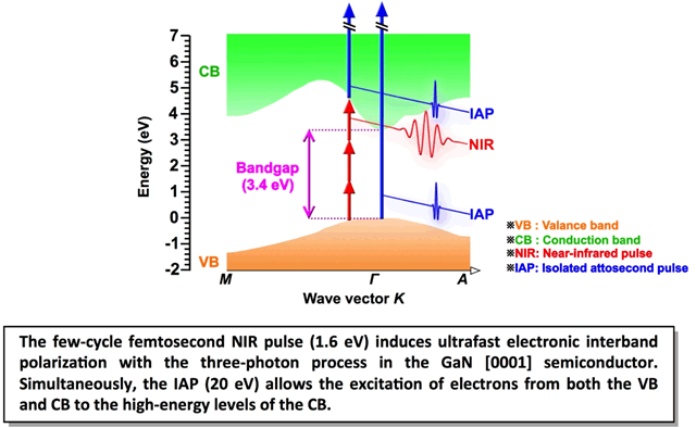
Fig.2:Transient absorption spectroscopy
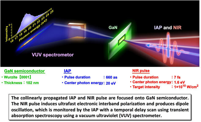
Fig.3:Transient absorption spectrum
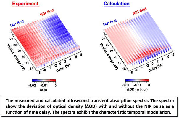
Fig.4:Dipole oscillation periodicity
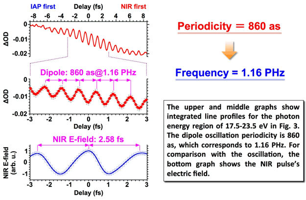
Fig.5:IAP generation
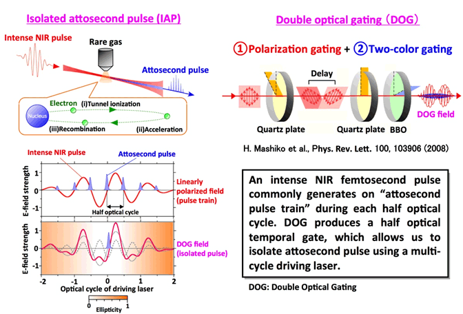
Fig.6:Attosecond streak method
1. Nippon Telegraph and Telephone (NTT) Corporation
Science and Core Technology Laboratory Group,
Public relations: a-info@lab.ntt.co.jp
2. Tokyo University of Science
Public relations: ura@admin.tus.ac.jp

Information is current as of the date of issue of the individual press release.
Please be advised that information may be outdated after that point.


NTT STORY
WEB media that thinks about the future with NTT