Microsoft ends support for Internet Explorer on June 16, 2022.
We recommend using one of the browsers listed below.
- Microsoft Edge(Latest version)
- Mozilla Firefox(Latest version)
- Google Chrome(Latest version)
- Apple Safari(Latest version)
Please contact your browser provider for download and installation instructions.


September 23, 2016
Generating High-speed Signals by using High-speed Electronic Devices and Signal Processing and Accomplishing 250-Gbps Short-distance Optical Transmission
--Anticipated as a technology leading to 1-Tbit-class optical transmission--
Nippon Telegraph and Telephone Corporation (NTT; Head Office: Chiyoda-ku, Tokyo; Hiroo Unoura, President and CEO) has successfully performed 250-Gbps (gigabits per second) short-distance optical transmission by means of a light-intensity modulation scheme (used by Ethernet, etc.) utilizing a new technology for generating high-speed signals by combining high-speed electronic devices and signal processing.
For short-distance optical transmission such as that provided by Ethernet, an intensity-modulation*1 scheme (which can be simply configured with optical components) is used. The speed of the CMOS*2 circuit in the output section of a digital signal-processing chip (for switching signal patterns in order to transform information being transmitted and modulate light) is limited, and it is difficult to create an intensity-modulated signal with speeds above that limit (namely, 250 Gbps).
Utilizing our original technology--called "DP-AM-DAC"--that doubles the speed of the output signal from a digital signal-processing chip, NTT has successfully generated a 250-Gbps signal by signal-intensity modulation and demonstrated 10-km 250-Gbps transmission in an optical transmission test using that signal. This accomplishment enabled 250-Gbps short-distance optical transmission using one wavelength, and by parallelizing such signal transmissions by using four wavelengths in the future, DP-AM-DAC shows potential as an optical-transmission technology for enabling short-distance large-capacity transmission at 1-Tbps (one terabit*3 per second), namely, a 10-times-higher transmission rate than that possible with currently standardized 100G Ethernet.
The proposed technology was presented at ECOC2016, an international conference held in Dusseldorf (Germany) on September 22nd (local time), as a "Post Deadline Paper" (namely, most-recent outstanding papers).
1.Background
For short-distance transmission such as that provided by Ethernet, transceivers must be low cost and compact as well as have low power consumption. In regard to conventional short-distance optical transmission, a simple modulation scheme called "intensity modulation", which utilizes one laser-light source and one light-detector with modulating the intensity of the optical signal only, is applied. As for optical transmission in recent times, complicated waveforms are used (for efficiently transmitting information), thereforea scheme that generates and transmits a signal by means of a digital processing chip is considered to be effective. A CMOS electronic circuit called a DAC*4, which is installed in the output portion of the chip so that it can convert the output of the digital processing chip to an analog signal, operates in a frequency band*5 in the order of 30 GHz; consequently, it is difficult to output the high-speed signal required by 250-Gbps-class transmission (which requires a wider frequency band, namely, above 60 GHz).
2.Achievements
By means of signal processing in the chip in a manner that is unaffected by the limited speed of the DAC (preliminary signal processing in Fig.1), the proposed DP-AM-DAC or "Digital-Preprocessed Analog-Multiplexed DAC technology" outputs the input signal as a two-system signal; namely, it is converted to a low-speed signal with speed below the limited speed of the DAC output. After that, a high-speed signal is created and the above-described bottleneck is eliminated by combining into one; a compound semiconductor*6 electronic circuit (AMUX*7) with the digital signal-processing circuit (thereby enabling higher-speed operation than a CMOS circuit connected externally to the digital signal-processing circuit). Moreover, as for spurious signals generated by the AMUX, it is possible to create proper high-speed signals by applying a method by which a two-line signal is configured by preliminary signal processing in a reverse operation that cancels out those signals when they are about to be generated. In the present study, DP-AM-DAC was used to create a frequency band of 60 GHz, and the world's first 250-Gbps 10-km optical transmission in that band was accomplished with an optical-intensity modulation called DMT*8, as used for ADSLs (see Figs. 2 and 3).
3.Future plans
In light of the success of this transmission test, application of DP-AM-DAC is expected to be expanded to various fields that require high-speed modulated signals, including large-capacity (e.g., 1-Tbps-class) short-distance optical communication based on multiplexing four wavelengths.
4.Technical features
Digital-Preprocessed analog-multiplexed DAC technology (DP-AM-DAC) --an original technology developed by NTT--doubles the speed of the signal output from a digital signal-processing chip. While the signal input into the digital signal-processing chip is parallelized within the chip, the input signal is crammed into the low-frequency range by shifting the signal in the high-frequency range or by a reverse operation to make the signals equal or below the speed limitation of the DAC (which is configured in the output portion of the digital signal-processing chip). As a result, degradation of the signal when it is output from the digital signal-processing chip is suppressed. Then, the parallelized output signals from the digital signal-processing chip are summed up to analog signals at high speed by the AMUX. In the frequency domain, taking the AMUX as a convolution operation of signals, the AMUX yields images of the signal on both sides of the switching clock frequency and it generates a high-frequency or high-speed signal. At that time, although spurious signals are also generated in the usual case, it is possible to obtain the desired signals only by preprocessing the digital signals so that the signals are reversely designed to cancel out the spurious signals through the AMUX operation. Since this technology uses both digital preprocessing and AMUX for digital analog conversion, we call it "Digital-Preprocessed Analog-Multiplexed DAC technology", or DP-AM-DAC.
Figure 1: Comparison of conventional technology and frequency-band-doubler technology
The digital signal-processing chip is composed of a DSP*9 and the DAC, and the frequency stated in the middle of the figure is the frequency band. To attain a transmission speed of 300 Gbps, a frequency band in the order of 60 GHz is required. However, the frequency band concerning the DAC portion is conventionally limited to about 30 GHz, so achieving transmission at 300 Gbps is impossible as is. When Digital-Preprocessed Analog-Multiplexed DAC technology is used to generate dual parallelized signals in frequency bands of 30 GHz, and the signals are combined by means of an AMUX, an overall frequency band of 60 GHz is created, and 300-Gbps transmission is possible.
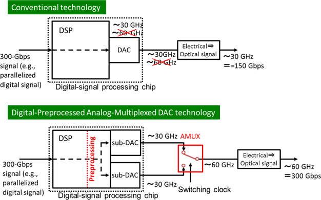
Figure 2: Configuration of transmission test
For the transmission test, the data is created by a PC simulating a digital signal-processing chip, and signals are generated by an arbitrary-waveform generator. These signals are combined by the Digital-Preprocessed Analog-Multiplexed DAC integrated with the in-house-developed AMUX, and the output is modulated by a wideband laser module (EADFB*10 laser) and then transmitted.
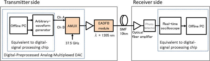
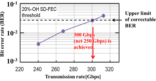
Figure 3: Results of transmission tests
Measured bit error rate (BER) is plotted against transmission speed in Fig. 3. The upper limit of the transmission speed is obtained from the point of intersection of the plotted line with the upper limit of BER (namely, maximum BER correctable by error-correcting code). According to this result, maximum transmission speed is 300 Gbps; however, net transmission speed (namely, that minus the contribution of the error-correcting code) is obtained as 250 Gbps.
Glossary:
-
Modulation:
Varying one or more properties of a waveform (in this study, a light wave) in order to transmit a signal. As for intensity modulation, the simplest case involves a signal with two intensity levels, one representing light on, and one representing light off. Multi-level intensity modulation is a scheme for transmitting signals by setting the brightness of the light wave at a level that allows a multitude of data to be transmitted at once. -
CMOS (complementary metal-oxide semiconductor):
As a structural component that creates a semiconductor integrated circuit, a CMOS is used to provide extensive functionality (such as that of a CPU). CMOS-type circuits are often used in the case of transmitting and receiving a large number of signals during large-capacity optical transmission. Although transmission speed of CMOS devices is being increased through device scaling, from the viewpoint of speediness, compound semiconductors are superior. -
1 Tbit (terabit) = 1000 Gbits (gigabits).
According to the present specification of 100-Gbit Ethernet, 25 Gbps (gigabits per second) × four wavelengths gives transmission speed of 100 Gbps. In the transmission test performed in this study, 250 Gbps was demonstrated, so by using four wavelengths (in accordance with the specification), data transmission at 1 Tbps (terabits per second) is possible. -
DAC (Digital Analog Converter):
A circuit for converting a digital signal (output from a digital signal-processing circuit) to an analog signal. -
Frequency band:
the range from the lowest frequency to the highest frequency needed to transmit a signal. In this study, the lowest frequency was set as the point of origin, so the frequency band is expressed by the highest frequency only. -
Compound semiconductor:
semiconductor material composed of a compound with multiple atoms. In this study, indium phosphide (InP) was used. In contrast to CMOS materials being suitable for large-scale circuits, compound semiconductors are suitable for integrated circuits with superior high-frequency properties. As for the result demonstrated in the transmission test, a circuit was constructed by using an InP hetero-junction bipolar-transistor integrated circuit developed at NTT Device Technology Labs. -
AMUX (analog multiplexer):
an electronic element that can rapidly switch an analog waveform without changing its form. -
DMT (discrete multi-tone):
a digital modulation scheme that enables efficient transmission by dividing the frequency band into multiple smaller frequency domains and allocating bit count in accordance with the transmission state at each frequency. -
DSP (digital signal processing) circuit:
A circuit used in recent years for generating and demodulating transmitted/received signals. -
EADFB (electro absorption distributed feedback) laser:
The abbreviated name for an electroabsorption-modulator-integrated distributed-feedback laser. It functions as an optical-source device in which one part for generating light with a single wavelength and another part for absorbing light and modulating it are integrated in a single semiconductor chip.
Contact information
Nippon Telegraph and Telephone Corporation
Science and Core Technology Laboratory Group, Public Relations
a-info@lab.ntt.co.jp

Information is current as of the date of issue of the individual press release.
Please be advised that information may be outdated after that point.
NTT STORY
WEB media that thinks about the future with NTT