Microsoft ends support for Internet Explorer on June 16, 2022.
We recommend using one of the browsers listed below.
- Microsoft Edge(Latest version)
- Mozilla Firefox(Latest version)
- Google Chrome(Latest version)
- Apple Safari(Latest version)
Please contact your browser provider for download and installation instructions.
February 7, 2017
Opening of Ultra-high-speed IC Technology Using an Advanced Compound Semiconductor Process
Nippon Telegraph and Telephone Corporation (NTT; Head office: Chiyoda, Tokyo; President and Chief Executive Officer: Hiroo Unoura) is going to open with ultra high-speed IC technology that involves the most advanced R&D processes for InP compound semiconductors, aiming for the further evolution of the technology through collaboration with partners.
Targeting higher capacity in telecommunications, NTT has been pushing forward for many years with R&D on ultra-high-speed IC technology that uses an InP compound semiconductor process that produces higher speeds and higher output than silicon semiconductors. With this process, we have already achieved high-speed data transmission of 2 GBps (gigabytes per second) with a compact terahertz wireless transmitter that is capable of transmitting at tens of gigabits per second using the 300 GHz band (May 26, 2016 news release). We have also demonstrated transmission at 250 Gbps (gigabits per second) with the technology (DP-AM-DAC or "Digital-Preprocessed Analog-Multiplexed DAC technology" ) that doubles the output signal speed of optical transmitters for future high-capacity, short distance communication in data centers, etc. (September 23, 2016 news release). We are now making our ultra-high-speed IC technology that is based on the InP compound semiconductor R&D process openly available to all partners.
We will continue to bring collaboration partners together and provide them with process design kits (PDK) to support the application of this leading-edge compound semiconductor R&D process for making IC devices and further advance ultra-high-speed IC technology while creating new services and new business based on those devices with our partners.
1.Background
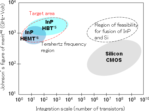
IC devices that use ordinary silicon technology can generally achieve high functionality through large-scale integration, as with CMOS*1 devices, but they are limited in speed and output. ICs that use InP*2 compounds, on the other hand, are less suitable for high degrees of integration, but they are capable of higher speeds and output than silicon devices. InP compound processes thus hold promise as a complementary device technology (Fig. 1). NTT is building a community of partners and making our leading-edge InP compound semiconductor process openly available to that community to advance the technology. Our specific objectives are to 1) develop new application areas for ultra-high-speed ICs and 2) work together with partners to achieve even higher speeds. The InP ultra-high-speed IC that we are making available cannot achieve the integration scale of a silicon CMOS. However, combination of the two technologies can open up new applications that provide both ultra-high speed and high functionality, qualities which are required for the post-Moore era*3 (Fig. 1).

2.Overview of the collaboration process
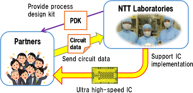
The opening of ultra-high-speed IC technology based on the leading-edge compound semiconductor R&D process involves the three specific activities listed below (Fig. 2).
- NTT provides the PDK*7 to all partners
- Partners use the PDK to design circuits
- NTT provides support for applying the leading-edge process to ICs
Through the above activities, we aim to work together with the community of partners to create new services and new business with ultra high-speed ICs and further develop the ultra high-speed IC technology.

3.Technical Points
Ultra-high-speed ICs can be implemented using our compound semiconductor R&D process, which features the world's highest level of operating speed. Examples of ultra-high-speed analog ICs that cannot be implemented with silicon technology include an IC that achieved double the bandwidth available with silicon technology by using InP HBT*5 that has an fT*8/fmax*9 characteristic of 400/450 GHz.
4.Future Plans
In 2017, we will conduct a trial and recruit partners. In 2018, we will begin to distribute the PDK to partners, and in 2019 we expect to prototype ICs using the leading-edge compound semiconductor process to begin.
Glossary
-
CMOS:
Complementary Metal Oxide Semiconductor, a structure for implementing semiconductor integrated circuits for CPUs and other devices that have large-scale functions; this type of circuit is often used in the transmission and reception of high-capacity optical signals. Higher speeds have been achieved by miniaturization, but compound semiconductors provide higher speed and higher output characteristics. -
InP:
Indium phosphide, a group III-V compound semiconductor that is used when implementing functions for applications that require high-speed and high-output. -
Post-Moore era:
The era in which semiconductor technology has advanced beyond Moore's Law. -
Johnson's figure of merit:
An index that represents semiconductor performance; higher values indicate higher speed and output characteristics. -
HBT:
Heterojunction Bipolar Transistor -
HEMT:
High Electron Mobility Transistor -
PDK:
Process Design Kit, a collection of information required in IC design -
fT:
Current gain cut-off frequency -
fmax:
Power gain cut-off frequency
Please direct inquiries to:
Nippon Telegraph and Telephone Corporation
Science and Core Technology Laboratory Group, Public Relations
a-info@lab.ntt.co.jp
Information is current as of the date of issue of the individual press release.
Please be advised that information may be outdated after that point.
NTT STORY
WEB media that thinks about the future with NTT


