Microsoft ends support for Internet Explorer on June 16, 2022.
We recommend using one of the browsers listed below.
- Microsoft Edge(Latest version)
- Mozilla Firefox(Latest version)
- Google Chrome(Latest version)
- Apple Safari(Latest version)
Please contact your browser provider for download and installation instructions.


March 14, 2017
Tokyo Institute of Technology
Nippon Telegraph and Telephone Corporation
Spin-resolved oscilloscope for charge and spin signals: Basic measuring instrument for future plasmonics and spintronics
(Tokyo, March 2017) Researchers at the Tokyo Institute of Technology (Tokyo Tech) and Nippon Telegraph and Telephone Corporation (NTT) have developed a "spin-resolved oscilloscope." This device is a basic measuring instrument for plasmonics and spintronics, which are key technologies for future electronics applications. The coupling of light and electronic charges in plasmonics will pave the way for ultra-high-speed information processing, whereas spintronics will provide low-energy-consumption technology in a highly information-oriented society. The spin-resolved oscilloscope pioneers future "spin-plasmonics," where ultra-high-speed low-energy-consumption devices will be achieved.
An electron has charge and spin, and both the charge- and spin-density excitations in an electronic system can be utilized in information processing. The dynamics of charge-density waves has been investigated in plasmonics, and that of spin-density waves has been studied in the field of spintronics. However, less effort has been devoted to combining these two technologies and to developing the expected ultra-high-speed and low-energy-consumption devices. To date, a major obstacle preventing the promotion of this research field has been the lack of a measuring instrument that is sensitive to both charge and spin.
In their recent paper, published in Nature Physics, Dr. Masayuki Hashisaka at Tokyo Tech and colleagues reported a "spin-resolved oscilloscope" that enables measurement of the waveforms of both charge and spin signals in electronic devices. An oscilloscope is a basic measuring instrument used in electronics; however, conventional oscilloscopes do not facilitate both charge and spin measurement.
The "charge signal" is the total charge of the spin-up and -down electron densities. Further, the "spin signal" is the difference between the spin-up and -down electron densities. Both these signals traveling in a semiconductor device can be detected by the spin-resolved oscilloscope, which is composed of a spin filter and nanometer-scale time-resolved charge detectors. The spin filter separates the spin-up and -down electrons, while the time-resolved charge detector measures the waveforms of the charge-density waves. By combining these spintronic and plasmonic devices, the spin-resolved oscilloscope is established.
Using this spin-resolved oscilloscope, Hashisaka and colleagues demonstrated waveform measurements of charge- and spin-density wavepackets in a semiconductor device. They succeeded in observing the spin-charge-separation process in a one-dimensional (1D) electronic system composed of quantum Hall edge channels, which is a prototypical system for the investigation of 1D electron dynamics. This was the first experiment in which a single spin-charge-separation waveform measurement allowed estimation of all the relevant system parameters. Further, this observation manifests not only the usefulness of the spin-resolved oscilloscope, but also the possibility for developing novel plasmonic and spintronic devices based on 1D semiconductor materials.
The spin-resolved oscilloscope will promote investigations in both plasmonics and spintronics; for example, this device will aid studies of electron dynamics in various 1D systems. In addition, the spin-resolved oscilloscope will pave the way for future "spin-plasmonics," where ultra-high-speed and low-energy-consumption devices will be achieved.
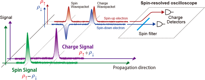 Figure. Conceptual diagram of charge- and spin signal measurement
The spin-resolved oscilloscope is established by combining spintronic and plasmonic devices, i.e., a spin filter and time-resolved charge detectors.
Credit: Masayuki Hashisaka
| Authors | : | M. Hashisaka1*, N. Hiyama1, T. Akiho2, K. Muraki2 and T. Fujisawa1* |
| Title of original paper | : | Waveform measurement of charge- and spin-density wavepackets in a chiral Tomonaga-Luttinger liquid |
| Journal | : | Nature Physics |
| DOI | : | dx.doi.org/10.1038/nphys4062 |
| Affiliations | : | 1Department of Physics, Tokyo Institute of Technology, 2-12-1-H81 Ookayama, Meguro, Tokyo 152-8551, Japan. 2NTT Basic Research Laboratories, NTT Corporation, 3-1 Morinosato-Wakamiya, Atsugi, Kanagawa 243-0198, Japan. |
Corresponding to: hashisaka@phys.titech.ac.jp; fujisawa@phys.titech.ac.jp
Contacts
Emiko Kawaguchi
Center for Public Affairs and Communications,
Tokyo Institute of Technology
E-mail: media@jim.titech.ac.jp
Tel: +81-3-5734-2975
Information is current as of the date of issue of the individual press release.
Please be advised that information may be outdated after that point.


NTT STORY
WEB media that thinks about the future with NTT