Microsoft ends support for Internet Explorer on June 16, 2022.
We recommend using one of the browsers listed below.
- Microsoft Edge(Latest version)
- Mozilla Firefox(Latest version)
- Google Chrome(Latest version)
- Apple Safari(Latest version)
Please contact your browser provider for download and installation instructions.


April 3, 2017
First demonstration of nanowire lasers at telecom wavelengths and high-speed signal modulation Novel method for integrating ultrasmall photonic devices on a silicon chip
Nippon Telegraph and Telephone Corporation (NTT; Head Office: Chiyoda-ku, Tokyo; President and CEO: Hiroo Unoura) has demonstrated the first sub-wavelength nanowire lasers at telecom wavelengths, which was enabled by placing a sub-wavelength semiconductor nanowire (*1) on a silicon photonic crystal (*2) to form an optical nanocavity (*3). NTT has also demonstrated high-speed signal modulation of nanowire lasers, which had not been achieved for nanowire lasers. This technology enables us to integrate a large number of nanophotonic devices based on nanowires with various functions, and is promising for realizing dense optical networks in a processor chip, which is expected to lead to ultrafast information communication technology (ICT) with small power consumption.
This result is published in the American science journal "APL Photonics" on April 3, 2017. This work has been partly supported by JSPS KAKENHI Grant No. 15H05735.
Summarized achievements
- (ⅰ)First demonstration of sub-wavelength nanowire lasers at telecom bands
- (ⅱ)First demonstration of high-speed signal modulation by nanowire lasers
- (ⅲ)Novel technology to integrate nanolasers within a silicon photonic circuit
1.Background
The energy consumption of information and communications technology (ICT) has been increasing year by year at an accelerating pace, and thus there is a strong demand to introduce novel technologies to reduce it drastically. As the bit rate goes up, the energy consumption of ICT becomes dominated by electric systems/components, such as routers, data centers and their processor chips. This is because the electrical signal transport becomes more energy-consuming when the bit rate goes up. This trend is becoming notable especially within a processor chip where most of the energy will soon be consumed by electric wiring and on-chip network management. To solve this forthcoming problem, it is expected that dense photonic networks will be integrated into a processor chip. This will require technologies to integrate ultrasmall lasers with substantially smaller energy consumption within silicon photonic circuits.
A key requirement to reduce the consumption energy is to reduce the active volume of lasers. Since semiconductor nanowires are mass-produced ultrasmall materials with various functions including optical gain, they have been considered as a promising candidate for ultrasmall lasers for the purpose described above. However, it is not easy to achieve lasing with sub-wavelength nanowires, and there has been no demonstration of high-speed signal modulation. This is because it is fundamentally difficult to confine light in a sub-wavelength nanowire. In addition, in order to integrate with silicon photonic circuits, the operation wavelength of the lasers should be at telecom wavelengths where silicon becomes transparent. But previous nanowire lasers are all lased at much shorter wavelengths, which is because the optical gain of semiconductors is generally small at telecom bands.
2.Achievements
NTT Nanophotonics Center (located in Atsugi, Japan) has fabricated a hybrid device combining a compound semiconductor nanowire (Fig. 1) and a silicon photonic crystal (Fig. 2) that has achieved lasing oscillation at telecom wavelengths with high-speed signal modulation. A photonic crystal is an artificially-made nanostructure with a periodic modulation of the refractive index, which is capable of strongly confining light into a small space. In this work, NTT has realized an optical nanocavity which confines light into a nanowire with the emission wavelength in the telecom band, by placing the nanowire in the slot of a photonic crystal (Fig. 3). Continuous-wave lasing oscillation of nanowires by optical pumping (*4) has been achieved at telecom wavelengths for the first time. In addition, high-speed signal modulation at 10 Gbps (gigabits per second) has been demonstrated.
This technology will enable us to integrate nanolasers in silicon photonic circuits, leading to a novel photonic integration method for introducing ultra-low power dense photonic networks into a processor chip.
[Experiments]
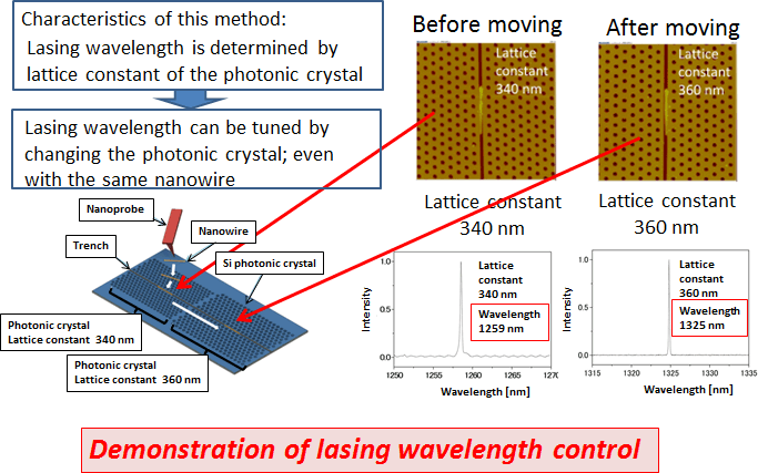
- (1)A silicon photonic crystal was prepared with semiconductor nanofabrication technology. A compound semiconductor (InAsP/InP) nanowire with a diameter of about 100 nm grown by a special crystal growth technique (vapor-liquid-solid method) was placed into a groove on the silicon photonic crystal by the nano-probe manipulation technique (Fig. 4), as explained below.
- (2)The fabricated device was optically pumped at cryogenic temperature. Unambiguous continuous-wave lasing oscillation was experimentally confirmed in their input-output characteristics, emission line width, and photon statics. (Fig. 5).
- (3)Then, the device was pumped by modulated light, and the high-speed signal modulation at 10 Gbps was observed by a highly-sensitive superconducting single photon detector (*5) (Fig. 6).
3.Future Plans
Next, we aim for integrating this nanowire laser coupled to a photonic crystal waveguide in the same chip, leading to applications in a photonic integrated circuit. We also aim for room-temperature current-driven lasing by optimizing the hybrid structural design, especially about the optical confinement factor. In addition, we plan to apply the same technique to realize other functional devices based on nanowires, such as photodetectors or switching devices.
As a final goal, we target photonic integrated circuits in which various functional nanophotonic devices are connected by waveguides in the same chip. By applying the present method, it will be possible to choose and place a certain nanowire having a certain function in a circuit to realize required functionality. This will greatly simplify the way we add functionalities to a photonic integrated circuit. We expect that if the present method is combined with sophisticated nanophotonic integration technologies, large-scale integrated photonic circuits will be realized and it will be possible to implement ultralow power dense photonic networks in a processor chip within 10 or 15 years, which will enable ultrahigh-speed ICT with substantially smaller energy consumption.
4.Technical Features
(1)Nanocavity formation with a nanowire and a photonic crystal
This work utilizes an interesting phenomenon in which a nanocavity can be formed simply by placing a sub-wavelength nanowire in the slot of a photonic crystal waveguide. NTT found and reported this phenomenon in 2014 (*7). The cavity formation mechanism is as follows. It has been well known that a small local structural modulation of a photonic crystal waveguide creates a nanocavity. Here, the placement of a sub-wavelength nanowire functions as the local modulation to the photonic crystal, thereby creating a nanocavity which strongly confine light into the nanowire. In this work, this mechanism is used to make a hybrid nanowire-photonic-crystal cavity which is used to as a laser resonator. This method enables exceptionally-strong light confinement into a sub-wavelength nanowire, which is one of the most important features of this work.
(2)Nanowires specialized for lasing
Semiconductor nanowires do not have sufficiently large gains at telecom wavelengths, thereby making it difficult to achieve lasing. In this work, nanowires with 100-layer multiple quantum wells were employed to maximize the gain. In addition, we carefully prepared nanowires whose emission polarization direction coincides with the polarization of the cavity mode. As a result of these optimizations, lasing oscillation at telecom wavelengths has been achieved.
(3)Placement of a nanowire by nano-probe manipulation
We have employed the nano-probe manipulation method to place a nanowire whose diameter is about 100 nm in a photonic crystal groove. For this method, we displace a single nanowire on a photonic crystal substrate to a certain desired position by scanning a nano-probe equipped in an atomic force microscope system (*6). By employing this technique, we have succeeded in displacing the nanowire from a certain photonic crystal to another photonic crystal with different lattice constant (Fig. 7). This result clearly shows that the lasing wavelength of the present nanowire lasers can be intentionally controlled by the host photonic crystal.
5.Publication
M. Takiguchi, A. Yokoo, K. Nozaki, M. D. Birowosuto, K. Tateno, G. Zhang, E. Kuramochi, A. Shinya, and M. Notomi, "Continuous-wave operation and 10-Gb/s direct modulation of InAsP/InP sub-wavelength nanowire laser on silicon photonic crystal," APL Photonics, 2, 046106 (2017).
Glossary
*1Semiconductor nanowire
A certain type of semiconductor crystal growth method, known as the vapor-liquid-solid method, can produce very thin wire-like structures whose diameter is 10 to 100 nm. It has been found that a large variety of semiconductors exhibits this growth mode, including compound semiconductors useful for photonic devices. It is possible to implement various functional structures into a nanowire during the growth, such as heterostructures and a current-injection junction.
*2Photonic crystal
An artificial structure whose refractive index is periodically modulated by a length scale comparable to the wavelength of light, usually fabricated by semiconductor lithography technology. Since photonic crystals behave as optical insulators, which do not exist in nature, extraordinarily strong light confinement becomes possible and they are therefore expected to realize ultrasmall photonic devices and circuits.
*3Optical nanocavity
An optical cavity is an element which confines light with a certain resonance. Since it is fundamentally difficult to confine light in a small space, miniaturization of high-performance cavities has been difficult. Historically, small cavities whose size is about 10 to 100 times of the wavelength of light have been called "microcavities". Recently, ultrasmall cavities whose size is comparable to the wavelength of light (the volume is less than 1 μm3) are called "nanocavities". Various high-performance nanocavities have been realized by employing photonic crystals.
*4Optical pumping
In order to achieve lasing, the active medium should be pumped up to excited levels with optical gain by optically or electrically pumping. In this work, the device was optically pumped by an external laser.
*5Superconducting single-photon detector
A very sensitive and fast photodetector employing a superconductor. Single photons can be detected because a single photon absorbed in the detector breaks the superconductive state.
*6Atomic force microscope
A microscope for measuring the surface shape of a sample by scanning the surface with a nano-probe so as to keep the atomic force between the probe and the sample surface constant. Nanometer resolution is achievable. In this study, the nano-probe equipped in an atomic force microscope is employed for manipulating and displacing a nanowire on the sample surface.
*7NTT news release
http://www.ntt.co.jp/news2014/1402e/140220a.html
Press Contact
Nippon Telegraph and Telephone CorporationScience and Core Technology Laboratory Group, Public Relations |
 NTT Has Instituted a Logo to Represent R&D Activities. |
Fig.1 Semiconductor nanowires
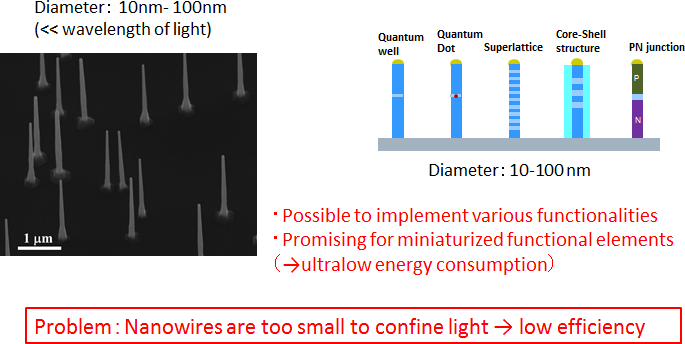
Fig.2 Photonic crystal
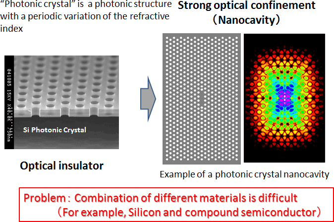
Fig.3 Nanowire-induced nanocavities
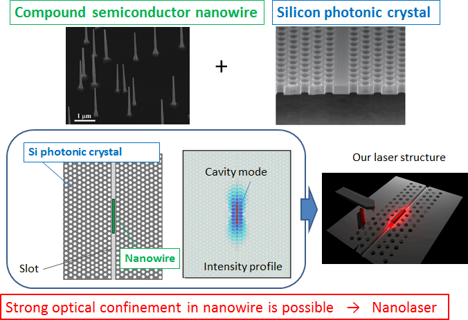
Fig.4 Fabrication of the nanowire laser
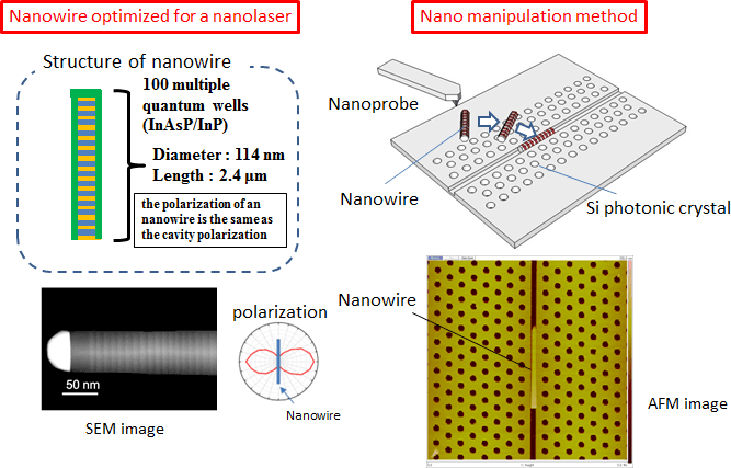
Fig.5 Lasing oscillation of a nanowire laser
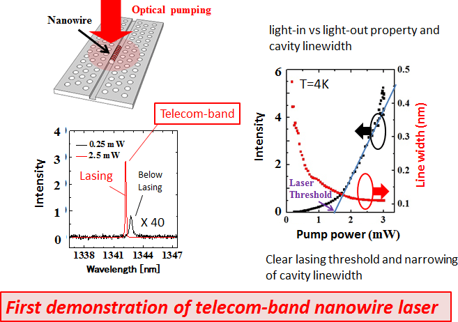
Fig.6 High-speed modulation of a nanowire laser
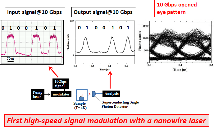
Fig.7 Control of lasing wavelength
Information is current as of the date of issue of the individual press release.
Please be advised that information may be outdated after that point.


NTT STORY
WEB media that thinks about the future with NTT