Microsoft ends support for Internet Explorer on June 16, 2022.
We recommend using one of the browsers listed below.
- Microsoft Edge(Latest version)
- Mozilla Firefox(Latest version)
- Google Chrome(Latest version)
- Apple Safari(Latest version)
Please contact your browser provider for download and installation instructions.


October 16, 2018
An ultra-high-speed IC capable of generating 256 Gbps PAM4 signals per lane Expected to facilitate a tenfold increase in the optical transmission capacity of datacenters compared with current levels
Nippon Telegraph and Telephone Corporation (NTT; Head office: Chiyoda-ku, Tokyo; President & CEO: Jun Sawada) has succeeded in combining a high-speed DAC (digital-to-analog converter) (*1) architecture with waveform quality enhancement technology to generate PAM4 (*2) coded signals (which are starting to be adopted in Ethernet and other networks) at a rate of 256 Gbps.
In Ethernet and other short-range optical communication technologies that are used in datacenters, intensity modulation (*3) schemes with a simple optical component configuration are used in order to satisfy energy-saving and economic requirements. A type of intensity modulation called PAM4 coding has recently grown in popularity as a way of meeting the demand for increased capacity. In PAM4 coding, the information to be transmitted must be transformed into multilevel analog voltages. However, it was found to be difficult to generate high-speed and high-quality multilevel voltage waveforms sufficient for 256 Gbps transmission.
At NTT, we have succeeded in generating 256 Gbps multilevel voltage signals (at a symbol rate of 128 Gbaud) by using InP (*4) -HBT (*5) to fabricate a PAM4 signal generator circuit incorporating our proprietary high-speed DAC architecture technology and waveform enhancement technology. We expect this ultra-high-speed IC technology will be used for short-range high-capacity communication in datacenters and other facilities, leading to the realization of transmission speeds of the order of 1 Tbps (*6), which is ten times faster than the 100 Gbps Ethernet technology that is currently in widespread use (based on 25 Gbps optical signals multiplexed across four lanes). Details of this technology are due to be presented at the IEEE BiCMOS and Compound Semiconductor Integrated Circuits and Technology Symposium (BCICTS 2018), to be held in San Diego, California, from 14th October.
1.Research background
Short-range communication technologies such as Ethernet are required for low-cost, compact low-power transceiver equipment in data centers and other such facilities. Conventional short-range communication uses a NRZ (non-return-to-zero) code that transmits data as a pulse signal with two levels. For higher transmission capacity, the use of PAM4 coding is being introduced. This is a modulation scheme where data is transmitted as a pulse signal with four levels (Fig. 1). In PAM4 coding, the transmitted data must be transformed into multilevel analog voltages, but it has been difficult to generate multilevel voltage waveforms of sufficient speed and quality for 256 Gbps transmissions.
2.What we have achieved
By using InP-HBT process technology (Fig. 4) together with our proprietary high-speed DAC architecture and waveform quality enhancement technology (Figs. 2, 3), we have succeeded in fabricating a PAM4 signal generator circuit capable of generating 256 Gbps multilevel voltage signals at a symbol rate of 128 Gbaud (Fig. 5). In 100 Gbps Ethernet technology, which is currently in widespread use, optical signals are multiplexed across four lanes, each with a capacity of 25 Gbps. By doubling the number of signal levels and increasing the signaling speed by a factor of five, we have succeeded in developing the world's first ultra-high-speed IC capable of generating PAM4 signals with a data rate of 256 Gbps per lane (ten times that of current practical technology) (Fig. 6).
3.Future prospects
This ultra-high-speed IC can generate high-quality multilevel voltage signals with a high symbol rate (128 Gbaud), which has so far been difficult to achieve. It is therefore expected to find applications in the R&D of innovative devices with symbol rates of 100 Gbaud to 128 Gbaud for next-generation large-capacity communication systems, and in measuring instrument (signal generators) for system verification. We also expect this technology to lead to developments in fields such as large-capacity optical communication that require high-speed multilevel signals and large-capacity optical communications, including four-lane multiplexing to achieve 1 Tbps transmission. At NTT, by cooperating with our partners, we aim to create new services and industries using ultra-high-speed ICs, and to promote the continued evolution of ultra-high-speed IC technology (*7).
4.Technical points
We have realized a PAM4 signal generator circuit (Fig. 2) by applying our proprietary high-speed DAC architecture technology and waveform enhancement technology. In general, DAC require that multi-bit digital signals are input at the same speed as the symbol rate of the generated analog signal, and this digital input interface has limited the operating speed of the DAC as a whole. Also, the operation of DACs at high speed has given rise to problems such as waveform distortion due to skew (temporal shifts) between bits inside the DAC, and noise due to leakage of the clock signal into the data signals.
In this technology, by applying our proprietary high-speed DAC architecture technology, which uses a high-speed selector circuit (SEL) to provide half-rate inputs, together with our waveform enhancement technology with a distortion compensation delay circuit and noise rejection buffer, we can dramatically improve the operating speed and waveform quality. Following the fabrication of a PAM4 signal generation circuit using our in-house InP-HBT technology, we have succeeded in generating multilevel voltage signals at a rate of 256 Gbps.
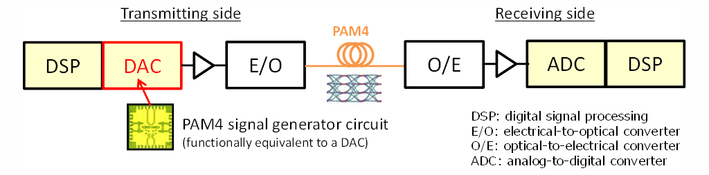 Fig. 1: Short distance optical transmitter configuration example
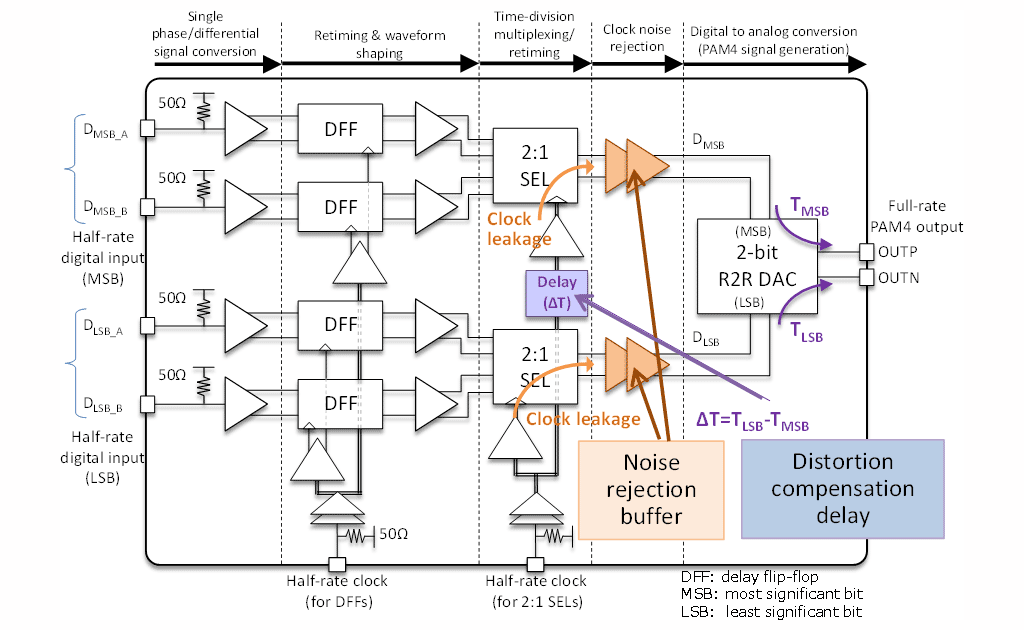 Fig. 2: PAM4 signal generator circuit configuration
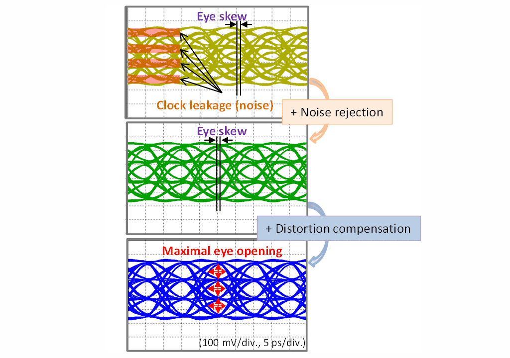 Fig. 3: Waveform simulation (200 Gbps)
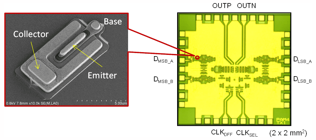 Fig. 4: PAM4 signal generator chip fabricated using our in-house InP HBT technology
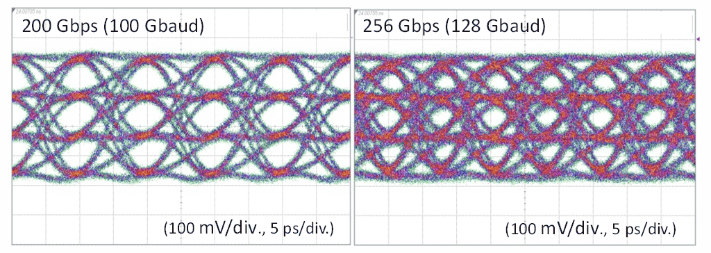 Fig. 5: Measurement of ultra-high-speed PAM4 signal generator waveform
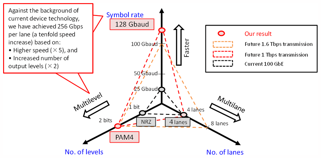 Fig. 6: Significance of this achievement
Glossary
*1DAC (Digital to Analog Converter):
A circuit that converts the digital signal output from a digital signal processing circuit into an analog signal.
*2PAM4 (4-level pulse amplitude modulation):
An intensity modulation scheme that transmits two bits of data (00, 01, 10, 11) at a time using four analog level pulse signals. Compared with a NRZ (non-return to zero) code that transmits a single bit of data (0, 1) via two analog level pulse signals, PAM4 can transmit twice as much information at a time.
*3Modulation:
Altering a waveform in order to send information. In the case of an electrical signal, for example, the simplest form of intensity modulation involves switching between binary voltage signals. In multilevel intensity modulation, more information is transmitted at a time by sending signals at several voltage levels so that more information can be sent at a time.
*4InP:
Indium phosphide. A Group Ⅲ-Ⅴ semiconductor consisting of indium and phosphorus, used when implementing functions for applications that require high speed and/or high output.
*5HBT:
Heterojunction bipolar transistor
*61 Tbps (1 terabit per second):
A data transfer rate 1,000 times faster than one gigabit per second (1 Gbps). The current 100 Gigabit Ethernet standard delivers 100 Gbps by combining 25 Gbps × 4 lanes. Our latest achievement has raised this limit to 256 Gbps, and allows 1 Tbps transmissions to be achieved by combining four lanes in the same way.
*7Press release, 7th February 2017:
"Opening of Ultra-high-speed IC Technology Using an Advanced Compound Semiconductor Process" (http://www.ntt.co.jp/news2017/1702e/170207a.html)
For further information
Science and Core Technology Group
Nippon Telegraph and Telephone Corporation
science_coretech-pr-ml@hco.ntt.co.jp
Tel: +81-46-240-5157
Information is current as of the date of issue of the individual press release.
Please be advised that information may be outdated after that point.


NTT STORY
WEB media that thinks about the future with NTT