Microsoft ends support for Internet Explorer on June 16, 2022.
We recommend using one of the browsers listed below.
- Microsoft Edge(Latest version)
- Mozilla Firefox(Latest version)
- Google Chrome(Latest version)
- Apple Safari(Latest version)
Please contact your browser provider for download and installation instructions.


March 7, 2019
Nippon Telegraph and Telephone Corporation
World’s first experimental long-distance WDM optical transmission at 1 Tbps per wavelength
Expected to provide large-capacity network communications for IoT and 5G services
Nippon Telegraph and Telephone Corporation (NTT, Head office: Chiyoda-ku Tokyo; President & CEO: Jun Sawada) has successfully performed the world’s first experimental long-distance transmission of optical signals by wavelength division multiplexing (WDM) at 1 terabit per second*1 per wavelength through the use of digital signal processing technology capable of precisely calibrating*2 multi-level signals and ultra-wideband optical front-end integrated device technology.
At NTT, we have developed ultra-wideband optical front-end integrated device technology and high-precision calibration technology for multi-level signals. Using this technology, we have succeeded in generating terabit-per-second signals (high-quality optical signals with multi-level modulation of 64QAM at a symbol rate of 120 gigabaud), and we have performed the world’s first successful transmission with 35 of these signals combined by wavelength division multiplexing for a distance of 800 km. This corresponds to a transmission speed ten times larger than the 100 gigabit-per-second capacity per wavelength of current practical long-distance systems, and this technology is expected to be useful for increasing the capacity of communication networks to support the spread of IoT and 5G services. Details of this technology will be announced at the Optical Networking and Communication Conference & Exhibition (OFC 2019) in San Diego, US from March 3.
1.Research background
With the spread of new information & communication services such as IoT and 5G, communication traffic is expected to continue increasing in the future, and there is also a need for additional capacity in backbone optical communication networks to be provided economically. From the viewpoint of economy, it is effective to increase the transmission capacity of each optical signal wavelength, and by increasing the symbol rate*3 of signals and increasing the number of bits per symbol,*4 we set ourselves the goal of achieving long-distance optical communication by using wavelength division multiplexing to combine multiple optical signals with a capacity of 1 terabit per second per wavelength.
To expand the transmission capacity per wavelength, it is necessary to overcome the speed limitations of silicon CMOS*5 semiconductor circuits. At NTT, we have hitherto been researching and developing integrated devices and optical transmission methods using bandwidth doubler technology*6 that uses AMUX*7 to break through the speed limit of silicon CMOS, and we have successfully generated optical signals with a symbol rate over 100 gigabaud. However, due to shortfalls in the technology available for optical front-end circuitry (such as loss variations due to signal paths and signal path length differences), it has been difficult to create optical multi-level signals of sufficient quality for wavelength-division multiplexed transmission over long distances and at high speeds of 1 terabit per second per wavelength.
2.What we have achieved
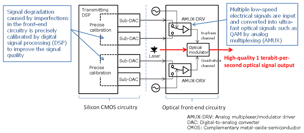
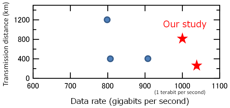
In this study, using digital signal processing technology capable of precisely calibrating multi-level signals and ultra-wideband optical front-end integrated device technology (Fig. 1), we successfully performed the world’s first experimental long-distance transmission of optical signals by wavelength division multiplexing (WDM) at 1 terabit per second*1 per wavelength. We achieved a symbol rate of 120 gigabaud by using AMUX fabricated with an in-house InP HBT*8 in the optical front-end circuitry, and we succeeded in generating PDM-PS-64 QAM*9 optical signals with multi-level modulation through the use of high precision calibration technology. We also achieved successful transmission of 35 wavelength-division multiplexed signals over 800 km (Fig. 2).
3.Future prospects
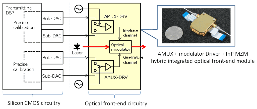
Since this technology makes it possible for the first time to generate high-quality 64QAM signals with a high symbol rate (120 gigabaud), it is expected to facilitate the realization of high-capacity WDM optical communication systems that can transmit data over long distances at a rate of 1 terabit per second per wavelength. This is ten times faster than the 100 gigabit per second per wavelength capacity of long-distance systems that are currently in use, and is expected to be useful for increasing the capacity of communication networks to support the spread of IoT and 5G services. We have also implemented a hybrid integrated optical front-end module (Fig. 3) with AMUX-DRVs and an optical modulator (InP MZMs*10), and we have successfully generated QPSK optical signals at up to 192 gigabaud and 8QAM optical signals at up to 160 gigabaud, which we expect to apply to optical transmission experiments in the future. We aim to further evolve this technology as fundamental building block of ultra-fast optical communication to break through the modulation speed limit of silicon CMOS.
4.Technical points
By introducing an AMUX analog multiplex function to the optical transmission circuitry, the required bandwidth of electrical signals between the two circuit blocks of the silicon CMOS circuitry and the optical transmission front end circuitry can be reduced by half compared with conventional equipment, making it easier to implement circuits. It is also able to generate optical signals with a symbol rate that exceeds the speed limit of silicon CMOS. Furthermore, by introducing our technology for calibrating the shortfalls of the optical transmitter front-end circuitry (such as loss variations due to signal paths and signal path length differences) with high precision, we have succeeded in generating high-quality optical signals with large numbers of modulation levels such as 64QAM, and transmitting of wavelength-division multiplexed signals over 800km.
Glossary
*1Terabit:
A quantity of data equal to 1,000 gigabits.
*2Calibration:
A digital signal processing techniques that compensate the impairment of optical components in transmitter and receiver for realizing the required overall system performance.
*3Symbol rate:
The number of times an optical waveform switches per second. A 120 gigabaud optical signal transmits information by switching the optical waveform 120 billion times every second.
*4Bits per symbol:
A number representing the amount of information conveyed by a single optical waveform. In 64QAM, a single optical waveform can take any of 64 (=26) different states, and can thus convey six bits of information.
*5CMOS (Complementary metal-oxide-semiconductor):
A semiconductor integrated circuit technology used for implementing CPUs and other large-scale functional circuits. This type of circuit is often used because it can handle large quantities of signals in the transmission and reception of large-capacity optical communications. Although the speed of CMOS circuits has been increased by miniaturization, compound semiconductor circuits are still faster.
*6Bandwidth doubler:
A technique that uses a combination of digital signal processing, two DACs and an AMUX to generate arbitrary signals at twice the bandwidth of each DAC.
*7AMUX (analog multiplexer):
An electronic circuit that alternately outputs two analog input signals by switching between them based on a clock signal.
*8InP HBT (InP heterojunction bipolar transistor):
A group III-V heterojunction bipolar transistor made using the elements indium and phosphorus. This type of transistor has superior switching speed and a high breakdown voltage.
*9PDM-PS-64QAM (polarization division multiplexed probabilistically shaped 64QAM):
PS-64QAM is a technique that achieves signal error rates asymptotic to the information theoretical limit by stochastically distributing the signal constellation of 64 levels in the electric field of the optical signal. By applying this technique to each of two independently polarized optical signals, it is possible generate a polarization division multiplexed (PDM) signal that further expands the transmission capacity.
*10InP MZM (InP Mach-Zehnder modulator):
A group III-V semiconductor Mach-Zehnder optical modulator made using the elements indium and phosphorus. Has excellent high-speed performance.
For inquiries regarding this press release
NTT Science and Core Technology Laboratory Group
Public Relations Office
science_coretech-pr-ml@hco.ntt.co.jp
TEL: 046-240-5157
Information is current as of the date of issue of the individual press release.
Please be advised that information may be outdated after that point.


NTT STORY
WEB media that thinks about the future with NTT