Microsoft ends support for Internet Explorer on June 16, 2022.
We recommend using one of the browsers listed below.
- Microsoft Edge(Latest version)
- Mozilla Firefox(Latest version)
- Google Chrome(Latest version)
- Apple Safari(Latest version)
Please contact your browser provider for download and installation instructions.


June 27, 2022
Nippon Telegraph and Telephone Corporation
Hokkaido University
World's First Attempt at Flexible Compensation Technique for Optical Power Difference Between Spatially Multiplexed Signals:
Milestone for Realizing Beyond 1-Peta-bit Class Large Capacity Optical Transmission Proposed in IOWN
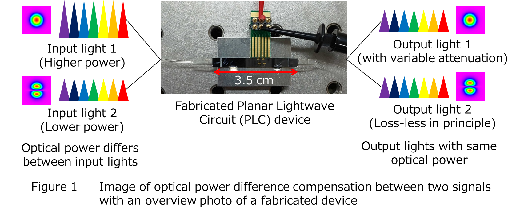
Nippon Telegraph and Telephone Corporation (NTT, Chiyoda-ku, Tokyo; President and CEO: Akira Shimada) and Hokkaido University (Kita-ku, Hokkaido; President: Kiyohiro Houkin) have succeeded in realizing a compact optical device which enables low loss, wideband and variable compensation of optical power difference between different kinds of signals (modes) for the first time in the world.
Mode division multiplexing within a single optical fiber is a candidate technology for future large capacity optical transmission. However, any optical power difference between modes increases at the end of the transmission line, because the attenuation coefficient in an optical fiber and amplification efficiency in an optical amplifier differs slightly between modes. The accumulated optical power difference is an impediment to realizing the mode multiplexing transmission system since it increases digital signal processing complexity in a receiver and severely restricts maximum transmission distance. We succeeded in compensating the optical power difference between modes ±0.5 dB or less by attenuating the specific mode selectively in a compact optical waveguide, namely the Planar Lightwave Circuit (PLC)*1. This compensation ability enables transmission distance extension of about 200 km per device.
This achievement is expected to be one of the key enablers for realizing an optical backbone network with more than 1 Peta-bit capacity, a target of Innovative Optical and Wireless Network (IOWN)*2 proposed by NTT.
This remarkable achievement will be presented at the European Conference on Optical Communication (ECOC) 2022, held in Basel (Switzerland) on 18-22 September 2022.
[Research Background]
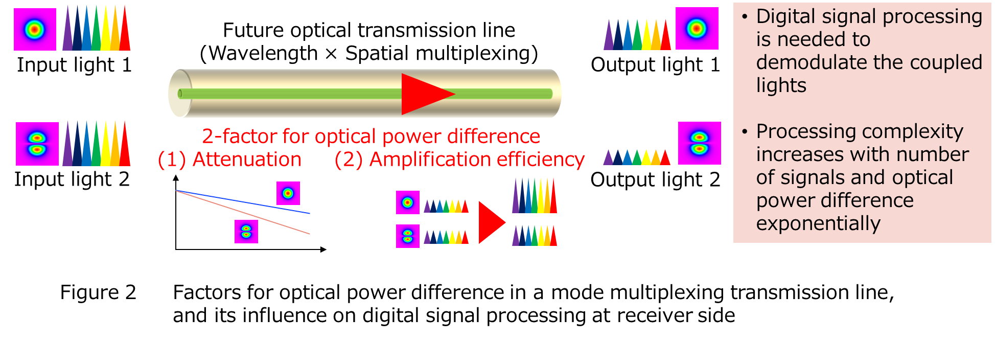
Mode division multiplexing can increase transmission capacity in proportion to the number of multiplexed modes. Hence, it is considered as one of candidate technology for realizing future large capacity optical backbone network. However, a slight difference in attenuation coefficient between modes accumulates across the transmission distance, as shown as (1) Attenuation in Fig. 2. Optical amplification efficiency also differs between modes and it results in the output power discrepancy of the amplifier, as shown as (2) Amplification efficiency in Fig. 2. Since the transmitted modes are randomly coupled in the transmission line, digital signal processing is needed to demodulate the received signals. However, the processing complexity increases exponentially in proportion to the number of multiplexed modes and optical power difference between modes. Moreover, the optical power difference between modes varies with the transmission distance and operation condition of the optical amplifier. Thus, a variable compensation technique for optical power difference among the modes is essential for realizing the mode multiplexing transmission system. However, there is currently no candidate technology which satisfies compactness, low loss and variability simultaneously.
[Features of Achievements]
By utilizing a planar lightwave circuit (PLC) technology which is superior for compactness and mass productivity, NTT realized, for the first time:
- Variable attenuation for a specific mode of two,
- Wideband amplification efficiency compensation in a two-mode optical amplifier.
1. Variable attenuation for a specific mode
Figure 3 shows the schematic of the proposed PLC configuration and operation principle. Our device consists of two cascaded optical power division/coupling circuits. A 50% of a specific mode which has higher optical power among the two is coupled from a bus waveguide to a delay line waveguide via the first optical power division circuit. A desired mode can be selected by designing a coupling length Lc and gap between waveguide g adequately. The light guided in the delay line waveguide is re-coupled into the bus waveguide via the second optical power coupling circuit. The coupled power varies depending on the delay time (phase difference) given in the delay line waveguide. Thus, the re-coupled (attenuating) power of the specific mode can vary by changing the refractive index of the delay line waveguide using a heater. Here, the other mode which has lower optical power has no excessive loss in principle since it simply passes through the bus waveguide. As a result, our device can realize compactness, low loss and variability simultaneously.
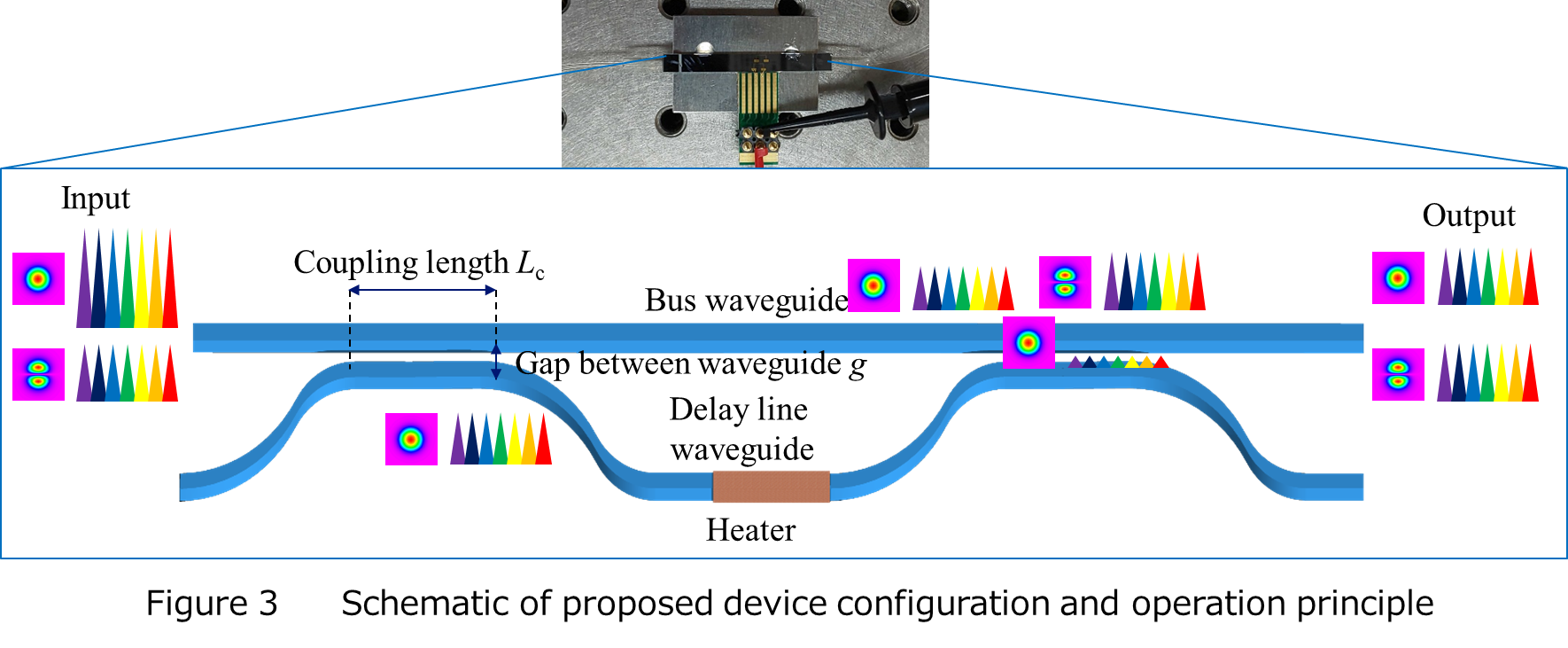
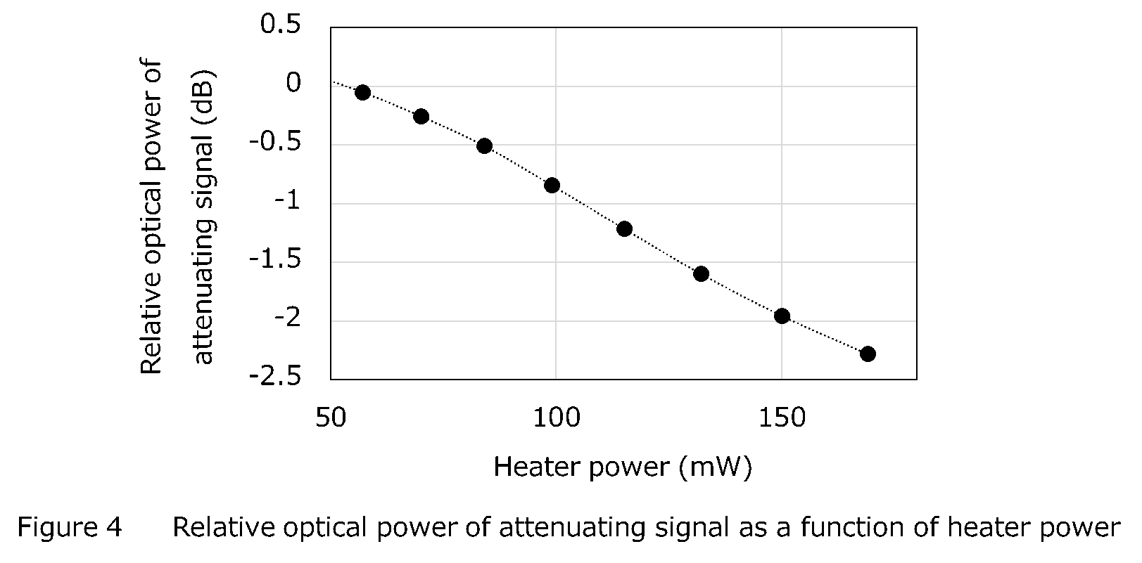
Figure 4 shows relative optical power of attenuating signal as a function of heater power. It can be seen that attenuation can be varied up to 2.3 dB by changing the heater power from 50 to 170 mW. Since a typical attenuation coefficient difference in a transmission line can be considered as less than 0.01 dB/km, the proposed device can compensate the optical power difference caused in a transmission line with more than 200 km long.
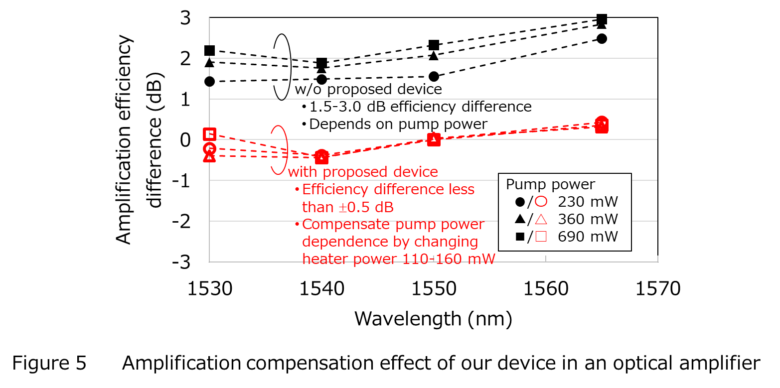
2. Wideband compensation of amplification efficiency difference
Figure 5 shows amplification efficiency difference measured with and without proposed devise. A two-mode optical amplifier for 1530 - 1565 nm wavelength region was used for this experiment. Black filled symbols show the results obtained without our device, and it shows that there are 1.5 dB or more amplifier efficiency difference over the entire operation wavelength. The amplifier efficiency difference without our PLC also depends on the operation condition of the amplifier. The operation condition means pump power, and which is shown with circles, triangles, and squares. An output power of the amplifier varies with the pump power. Red open symbols show the results obtained when we used proposed PLC device, and the results show that the amplification efficiency difference is successfully reduced to less than ±0.5 dB at all operation conditions without any noticeable influence on the wavelength dependence.
[Future Prospects]
The present achievement can be considered as an enabling technology for a large-capacity optical transmission line which uses mode division multiplexing. Our results make substantial progress in mode multiplexed optical transmission technology, together with our previous report on "Optical Transmission Property Control by Optimizing Optical Cable Structure"*3. Effective use of spatial multiplexing is mandatory for realizing a supra-1-Petabit class optical transmission backbone as a target of IOWN*2 proposed by NTT. We will continue our industry-academia collaboration research on effective use on the spatial modes.
[Glossary]
*1PLC (Planar Lightwave Circuit)
Silica glass based optical waveguide technology which has been developed by NTT. PLC is superior to mass-production since the fabrication process is similar to the large scale integration.
*2IOWN (Innovative Optical and Wireless Network)
IOWN is a future communications infrastructure to promote a smart world by using cutting-edge technologies such as photonics and computing technologies.
*3Optical Transmission Property Control by Optimizing Optical Cable Structure
https://group.ntt/en/newsrelease/2020/03/09/200309a.html
Contact Information
Nippon Telegraph and Telephone Corporation
Information Network Laboratory Group
Planning Department, Public Relations Section
E-mail: nttrd-pr@ml.ntt.com
Hokkaido University
<1> Researcher
Prof. Kunimasa Saitoh
Graduate School of Information Science and Technology
Email: ksaitoh@ist.hokudai.ac.jp
<2> Media Contact
Public Relations Division
Department of Public Engagement
Hokkaido University
Email: en-press@general.hokudai.ac.jp
Information is current as of the date of issue of the individual press release.
Please be advised that information may be outdated after that point.


NTT STORY
WEB media that thinks about the future with NTT