Microsoft ends support for Internet Explorer on June 16, 2022.
We recommend using one of the browsers listed below.
- Microsoft Edge(Latest version)
- Mozilla Firefox(Latest version)
- Google Chrome(Latest version)
- Apple Safari(Latest version)
Please contact your browser provider for download and installation instructions.


March 12, 2026
NTT, Inc.
NTT Develops World's First Photodetector Combining 200-GHz-Class Speed and High Reliability for Next-Generation Optical Communications
— Advancing the realization of ultrafast optical communications for data center interconnects of 3.2-Tbps and beyond —
News Highlights:
- As demand grows for ultrahigh-speed optical communications in applications such as data centers, the world's first practical demonstration of a photodetector with a 200-GHz-class operating speed has been demonstrated. In addition, the device demonstrates the world's highest responsivity at this operating speed.
- Through the development of new device structures and technologies, including integrated semiconductor lenses within the device, high-speed operation, high reliability, and ease of manufacturing have been simultaneously achieved.
- This technology will contribute to advancing ultrafast measurement technologies that are essential for the research and development of high-speed optical communication devices. Looking ahead to next-generation communication speeds of 3.2 Tbps beyond the expected 1.6 Tbps, it is also expected to support the future development of optical transceivers operating at 3.2 Tbps and beyond.
TOKYO — March 12, 2026 — NTT, Inc. (Headquarters: Chiyoda-ku, Tokyo; President and CEO: Akira Shimada; hereinafter "NTT") has developed the world's first photodetector with a 200-GHz-class performance suitable for 400-Gbaud (*1) signals that achieves commercially relevant reliability.
Driven by advances such as parallel processing in computing, the speed of optical communications within data centers continues to increase. Photodetectors capable of operating at 200-Gbaud-class and above are a key technology for enabling this higher speed. However, existing technologies have faced challenges such as degraded sensitivity and reduced reliability as operating speeds increase. The newly developed technology achieved the world's highest combination of speed and responsivity in the 1310-nm wavelength band used for optical communications within data centers. In addition, assuming high-temperature environments inside server racks in data centers, the device demonstrated unprecedented long-term reliability equivalent to 50 years of operation under 85℃ conditions for photodetectors in the 200-Gbaud-class and beyond. This technology is expected to serve as a fundamental technology for optical transceivers in the 200-Gbaud to 400-Gbaud-class, which are essential for realizing communication speeds exceeding 3.2 Tbps (*2).
These research and development results will be presented as a top-scored paper, the highest evaluation by peer reviewers, at The 2026 Optical Fiber Communication Conference and Exhibition (OFC 2026), the world's largest international conference in the field of optical communications, to be held in Los Angeles, USA, from March 15 to 19, 2026. Building on these results, NTT will further advance development toward commercialization.
Background
Global communication traffic is rapidly increasing due to the growing use of parallel processing in computing and the widespread adoption of video streaming services. At the same time, the power consumption of data centers that operate these services is also rising sharply, becoming a significant societal issue. To process increasing volumes of traffic while suppressing power consumption, demand for high-speed optical communications is growing rapidly. In particular, for short-reach connections such as links between computer racks, Ethernet with capacities on the order of 3.2 Tbps is currently under discussion (*3).
At present, deployment is progressing for 800-Gbps Ethernet using transmitters and receivers with signal speeds (symbol rate) of 100 Gbaud. However, future Ethernet systems exceeding 3.2 Tbps will require signal speeds in the 200-Gbaud- to 400-Gbaud-class optical transceivers. Realizing optical communication beyond 200 Gbaud requires ultrafast transmitters and receivers capable of supporting these speeds. However, evaluating the signal quality of such systems is difficult with existing receivers and 100-GHz-class measurement instruments. Therefore, high-speed photodetectors are essential not only as measurement technologies for the development of next-generation transmitters but also as foundational technologies for realizing optical transceivers that exceed 3.2-Tbps transmission rates.
As photodetectors become faster, their device size must be reduced. This is because reducing the device capacitance allows signals to rise and fall more quickly, enabling the device to follow high-speed signals. However, shrinking the photosensitive region leads to reduced responsivity, which determines communication signal quality, as well as decreased long-term reliability, which indicates the device's operational lifetime. Achieving photodetectors that simultaneously provide high speed, high responsivity, and high reliability therefore remains a major challenge for sustaining optical communications in practical networks over long periods of operation.
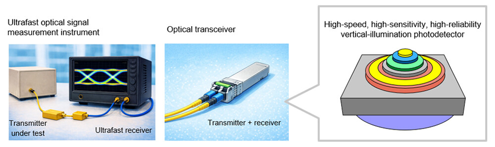 Figure 1 Application scenarios for the photodetector technology developed in this study
Research Results
In this study, a photodetector combining an operating speed exceeding 200 GHz with long-term reliability suitable for practical use was developed. This was achieved through a structural design that integrates three key technologies: an interference-based vertical-illumination structure that enhances responsivity, a stepped inverted structure that improves reliability, and a semiconductor lens integration technology that reduces manufacturing costs. Demonstrating practical-level long-term reliability in an ultrafast photodetector represents a world-first achievement. In addition, the device achieved the world's highest responsivity for ultrafast operation exceeding 200 GHz at the 1310-nm wavelength band used in data centers, with a responsivity–bandwidth product of 115 GHz·A/W (Figure 2(a)).
The developed device has an operating speed capable of supporting 400-Gbaud-class signals. However, generating and evaluating signals at this speed remains difficult with existing measurement technologies. Therefore, a demonstration experiment was conducted at 200 Gbaud, the highest level currently feasible with available measurement techniques (Figure 2(b)). Signal quality was evaluated using an eye diagram created by superimposing multiple received signal waveforms. The wide opening of the eye confirmed high-quality signal transmission.
To evaluate device reliability, accelerated degradation testing was conducted by heating the device to high temperatures, thereby accelerating material and structural degradation, and monitoring changes in the dark current (*4), defined as the current measured without optical input and used as a failure criterion. In accordance with the Telcordia GR-468-CORE specification (*5) for optical communication devices, 25 devices were randomly selected and subjected to a high-temperature operating test at 200℃ for 2,000 hours. The results confirmed extremely small variations among devices and minimal changes in dark current over time. Converting these results to the 85℃ operating temperature required for data center environments, the Arrhenius equation (*6), commonly used in reliability evaluation, indicates an expected device lifetime exceeding 50 years (Figure 2(c)).
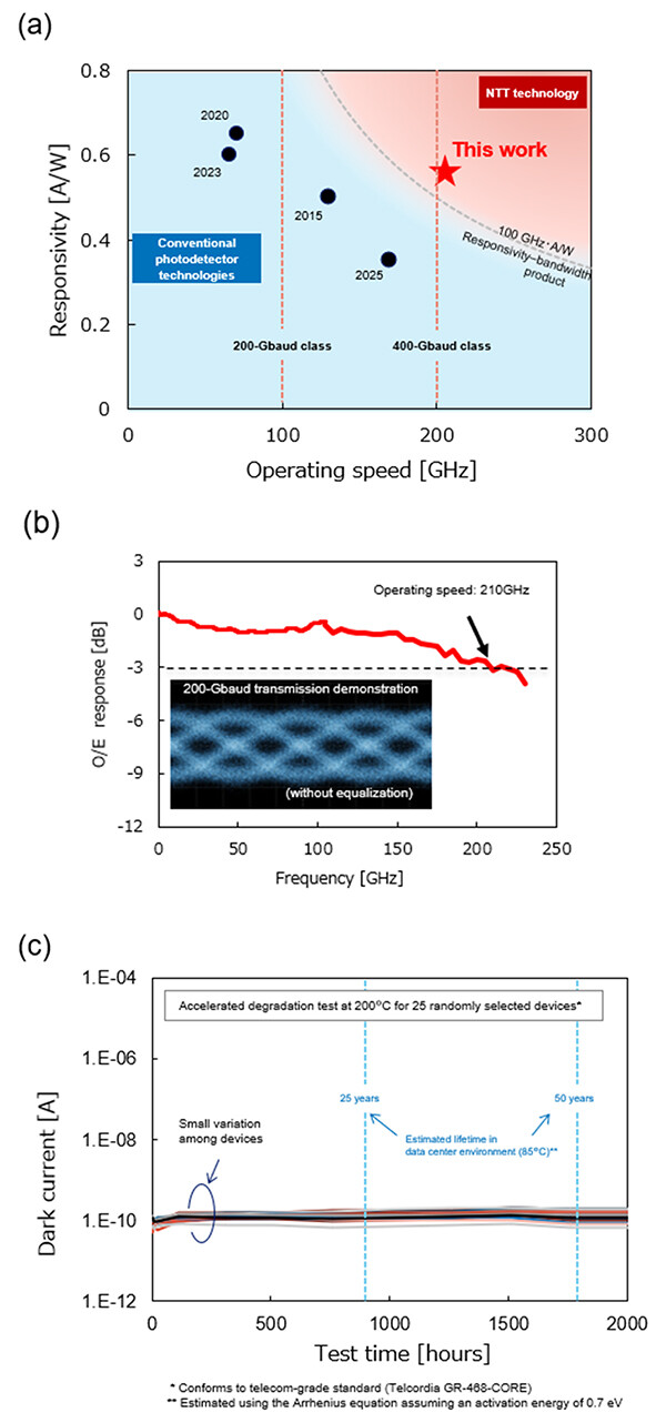 Figure 2
(a) Comparison with conventional photodetectors
(b) High-frequency characteristics and transmission experiment
(c) Long-term reliability evaluation results
Technical Highlights
(1) Interference-based vertical-illumination structure for enhanced responsivity
Increasing the speed and responsivity of photodetectors generally involves a trade-off. When the optical absorption layer is made thinner, the time required for photo-generated carriers to reach the electrodes (signal response time) becomes shorter, enabling higher-speed operation. However, thinner layers absorb less light, which reduces responsivity. For this reason, waveguide-type photodetectors (*7), which allow light to be absorbed over a longer distance and thus maintain higher responsivity, have traditionally been used for high-speed communications. However, these structures tend to be complex and can pose challenges such as reduced reliability.
In contrast, vertical-illumination photodetectors (*8) offer simpler structures and higher reliability, but ensuring sufficient responsivity has been a challenge. By further advancing NTT's long-established device design technologies (*9) and optimizing both optical design and band structure simultaneously, a vertical-illumination structure was developed that enhances responsivity by confining light through interference (Figure 3(a)). Using this technology, the world's highest responsivity was achieved for a 200-GHz-class photodetector operating at a wavelength of 1310 nm.
(2) Stepped inverted structure to improve reliability
Miniaturization of photodetectors is essential for increasing operating speed. However, as device size decreases, the density of dark current flowing along the device sidewalls, which are more susceptible to degradation, increases and can lead to device failure. Dark current is a representative indicator used to evaluate device degradation and typically increases as deterioration progresses. In general, the lower the initial dark current, the easier it is to suppress its increase over time, which is advantageous for improving long-term reliability.
NTT developed an inverted device structure that confines the active region within the interior of the device, thereby suppressing sidewall dark current (Figure 3(b)). This structure significantly increases the process difficulty for crystal growth and device fabrication. However, it was made possible by NTT's accumulated expertise from advancing the practical deployment of avalanche photodiodes (APDs) (*10) based on inverted structures. While typical photodetectors exhibit dark currents on the order of nA (10-9 A), this technology reduces the initial dark current to the pA level (10-12 A), among the lowest reported worldwide, thereby establishing high device reliability.
(3) Semiconductor lens integration on the backside to reduce manufacturing cost
Miniaturization is also essential for achieving higher operating speeds. To obtain high responsivity, the photosensitive region of the photodetector must be precisely aligned with the position where the optical signal is incident. Achieving this alignment during transceiver assembly requires highly precise positioning technology to minimize misalignment, which increases manufacturing costs.
NTT developed a technology that integrates a convex semiconductor lens directly into the photodetector, effectively enlarging the optical acceptance region and improving alignment tolerance. Fabricating a spherical lens structure in a semiconductor requires extremely high etching precision (*11). By leveraging NTT's accumulated expertise in high-precision etching of compound semiconductors, semiconductor lenses were successfully integrated into the photodetector structure (Figure 3(c)).
Using this technology, the tolerance for optical alignment was improved by more than twofold, enabling more efficient and lower-cost assembly of optical transceivers.
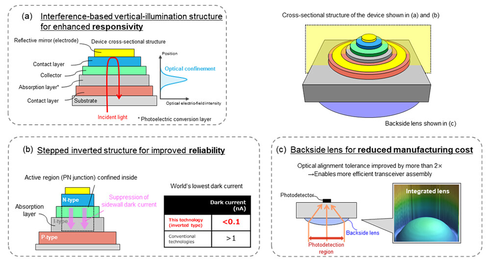 Figure 3 Key technologies of the proposed device
Future Outlook
NTT will continue to advance the development of various high-speed devices utilizing this photodetector technology to enable 3.2-Tbps optical communications. In addition, NTT Innovative Devices Corporation plans to promote the commercialization of this technology.
[Glossary]
- baud:
In serial communications, it represents the number of signal modulations (state changes) that occur per second. It is used as an indicator of communication speed, with higher values enabling faster communication. In contrast, hertz represents the frequency bandwidth that a photodetector or circuit can follow. Both are important indicators for achieving higher-speed communications. - 3.2-Tbps Ethernet and baud rate:
Bits per second indicate the amount of information (bits) that can be transmitted in one second. In the commonly used PAM-4 modulation format, one signal can represent two bits of information. Therefore, 200-Gbaud PAM-4 corresponds to 400 Gbps per wavelength (per lane), and 400-Gbaud PAM-4 corresponds to 800 Gbps per wavelength. As a result, 3.2-Tbps communication can be achieved, for example, by transmitting signals simultaneously using eight wavelengths with 200-Gbaud PAM-4 or four wavelengths with 400-Gbaud PAM-4. For the same overall data rate, using higher baud rates such as 400 Gbaud reduces the number of wavelengths required, which helps reduce the scale and cost of transmitters, (de)multiplexers (devices that combine or separate signals), and receivers. - Roadmap created by the Ethernet Alliance:
https://ethernetalliance.org/wp-content/uploads/2025/12/EthernetRoadmap-2026-Side1-2-Final-2-RGB.pdf
- Dark current:
The current that flows when a reverse bias is applied to a photodetector without optical input. It mainly originates from defects and is commonly used as an indicator of device degradation and failure. - Telcordia GR-468-CORE:
A comprehensive industry standard for ensuring the reliability of optoelectronic devices used in communication equipment, such as laser diodes, optical amplifiers, and photodiodes. It specifies conditions and evaluation methods for mechanical strength (e.g., vibration and shock), environmental resistance (e.g., temperature cycling and high temperature/high humidity), and lifetime testing, and defines pass criteria to ensure long-term stable operation of products. - Arrhenius equation:
A formula that describes the rate of chemical reactions. Because reaction rates depend on temperature, testing devices at high temperatures accelerates degradation processes, enabling estimation of the time to failure. - Waveguide-type photodetector:
A structure in which light enters from the side and propagates through a horizontally extended layer called a waveguide, typically made of compound semiconductors, where it is gradually absorbed and converted into an electrical signal. - Vertical-illumination photodetector:
A structure in which light is incident perpendicular to the surface or backside of the semiconductor substrate. Because it provides a large effective receiving area and enables easier packaging, it is widely used. - Ultrafast and high-sensitivity photodetector technologies
NTT Technical Journal:
https://journal.ntt.co.jp/backnumber2/1210/files/jn201210057.pdf (Japanese)
Single-travelling-carrier photodiode and its applications (The Optical Society of Japan, Kogaku):
https://annex.jsap.or.jp/photonics/kogaku/public/35-01-kaisetsu2.pdf (Japanese) - Avalanche photodiode (APD):
A type of photodetector used in high-sensitivity receivers. It utilizes impact ionization (avalanche multiplication) of carriers under reverse bias to achieve internal gain, enabling highly sensitive detection of weak optical signals. - Etching precision:
In semiconductor fabrication, the accuracy with which shapes created by etching (such as curvature, depth, position, and sidewall angles) match the design specifications. It affects the optical characteristics, reproducibility, and manufacturing yield of structures such as lenses.
About NTT
NTT is a leading global technology innovator, providing a broad range of services to both consumers and businesses. As a mobile operator and provider of infrastructure, networks, and services, NTT is dedicated to promoting a sustainable future through cutting-edge innovations. Our portfolio includes business consulting, AI-powered solutions, application services, global networks, cybersecurity, data center and edge computing, all supported by our deep global industry expertise. Generating over $90 billion in revenue and employing 340,000 professionals, we allocate 30% of our annual profits to fundamental research and development. With operations spanning more than 70 countries and regions, our clients include over 75% of Fortune Global 100 companies, alongside thousands of enterprises, government organizations, and millions of consumers.
Media Contact
NTT, Inc.
NTT Science and Core Technology Laboratory Group
Public Relations
Inquiry Form![]()
Information is current as of the date of issue of the individual press release.
Please be advised that information may be outdated after that point.


NTT STORY
WEB media that thinks about the future with NTT