Microsoft ends support for Internet Explorer on June 16, 2022.
We recommend using one of the browsers listed below.
- Microsoft Edge(Latest version)
- Mozilla Firefox(Latest version)
- Google Chrome(Latest version)
- Apple Safari(Latest version)
Please contact your browser provider for download and installation instructions.



August 25, 2026
NTT, Inc.
NTT Advances AI for Science with an Interpretable AI-Driven Lab Approach
~From autonomous experiments using robots and machine learning to human-usable rules for semiconductor thin-film growth~
Key Points:
- NTT has developed a self-driving thin-film growth platform that integrates AI and robotic technologies, accelerating the cycle of thin-film growth and evaluation by approximately three times compared with conventional experiments conducted by engineers and researchers. Using this platform, NTT successfully fabricated a high-quality single-crystalline thin film of the ultra-wide-bandgap semiconductor β-Ga₂O₃ (beta gallium oxide). In addition to identifying optimal growth conditions, the platform extracted growth rules that can be understood and applied by researchers.
- This platform provides a foundation for a next-generation AI-driven lab that advances autonomous experimentation beyond simple "black-box optimization" toward the creation of scientific knowledge.
- The technology is expected to significantly improve the efficiency of developing new materials and semiconductors and accelerate the practical application of high-performance power semiconductors, contributing to an energy-efficient society and next-generation electronic devices.
TOKYO, August 25, 2026 — NTT, Inc. (NTT) has demonstrated "interpretable self-driving thin-film growth*1," which uses AI and automation technologies to autonomously optimize thin-film growth and convert the data obtained during the process into growth rules that can be understood and applied by researchers. The technology establishes a closed-loop optimization process that repeatedly performs thin-film growth and evaluation and determines the conditions for the next growth run. This enables the experimental cycle to be conducted approximately three times faster than conventional experiments operated by engineers and researchers. Using this technology, NTT successfully realized single-crystalline β-Ga₂O₃*2 homoepitaxy by sputtering*3, which had not been previously reported. β-Ga₂O₃ is one of the next-generation power semiconductor materials. In addition, AI analysis was used to extract growth rules for improving thin-film quality, and their effectiveness was confirmed through re-optimization. This achievement expands "AI for Science"*4, which uses AI to advance and accelerate scientific research, from simply searching for optimal conditions to the creation of scientific knowledge.
The research results were published in Nature Communications on August 13, 2026.
Background
In recent years, "AI for Science," which uses AI and automation technologies to advance and accelerate scientific research, has attracted increasing attention. In materials research, efforts are also underway to efficiently explore experimental conditions using machine learning. In particular, efficient exploration of growth conditions is important for thin-film growth, which plays a critical role in determining semiconductor material performance, because a wide range of conditions, including temperature and gas flow rates, affect thin-film quality.
NTT has been developing highly efficient thin-film growth technologies using AI, including the growth of high-quality oxide thin films such as SrRuO₃ using Bayesian optimization*5 and the automated derivation of growth conditions for compound semiconductors by incorporating knowledge of semiconductor properties.
However, while conventional AI-based condition searches can identify optimal conditions, the data obtained during the optimization process are effectively treated as a black box. As a result, it is difficult for researchers to understand why certain conditions are optimal and to apply the knowledge gained to other material systems or thin-film growth equipment.
To address this challenge, NTT has demonstrated "interpretable self-driving thin-film growth," which not only autonomously optimizes growth conditions but also extracts growth rules that can be understood and applied by researchers from the data obtained during the optimization process (Figure 1).
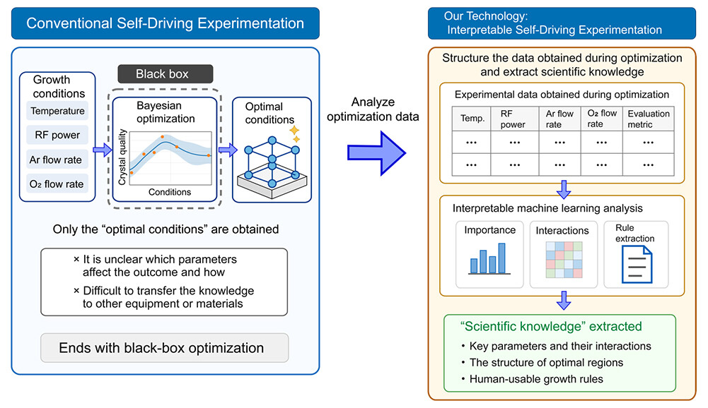 Figure 1. Overview of interpretable self-driving thin-film growth.
While conventional autonomous experimentation has focused primarily on searching for optimal conditions, this technology uses AI to analyze data obtained during the optimization process and extracts growth rules that can be understood and applied by researchers.
Key Technical Points
1. Self-driving sputter growth platform integrating automated growth, automated evaluation, and AI-based optimization
NTT has developed a self-driving sputter growth platform that integrates automated sputtering, automated optical evaluation, and AI-based optimization using Bayesian optimization. The platform establishes a semi-autonomous closed loop that repeatedly performs thin-film growth, evaluation, and determination of the conditions for the next growth process without human intervention in decision-making or data analysis (Figure 2).
Within the sputtering system, wafers used for thin-film growth are automatically transferred, and thin films are grown under the temperature, RF sputtering power, Ar (argon) flow rate, and O₂ (oxygen) flow rate conditions proposed by Bayesian optimization. After growth, thin-film quality is automatically analyzed and evaluated based on data obtained through automated optical measurements. The resulting evaluation is used to update the prediction model, and the conditions for the next growth run are automatically selected.
This accelerated the thin-film growth and evaluation cycle by approximately three times compared with conventional experiments operated by engineers and researchers. In addition, the use of Bayesian optimization enabled efficient and precise exploration of a multidimensional thin-film growth parameter space.
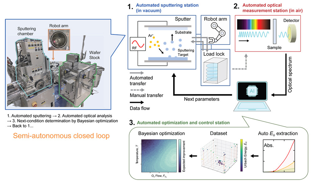 Figure 2. Overview of the self-driving sputter growth platform
2. AI analysis that converts optimization data into human-usable growth rules
In conventional autonomous experimentation, even when AI identifies optimal conditions, it is difficult for researchers to understand why those conditions are optimal and use the resulting knowledge in other materials or equipment.
To address this challenge, NTT analyzed the growth-condition and thin-film-quality data obtained through the self-driving closed loop using random forest*6, an ensemble machine learning method that combines multiple predictive models. By decomposing the predictions generated by the random forest into the contributions of individual growth parameters and interactions between parameters, NTT identified how each growth parameter affects thin-film quality, how the parameters interact with one another, and the structure of the optimal region.
This made it possible to distill complex, multidimensional optimization results into growth rules that can be understood and applied by researchers. By integrating autonomous experimental exploration with the extraction of growth rules, this technology provides a foundation for a next-generation AI-driven lab that advances from searching for experimental conditions to creating scientific knowledge.
Experimental Overview
1. Realization of single-crystalline β-Ga₂O₃ thin films
As a material for demonstrating the technology, NTT selected β-Ga₂O₃, one of the next-generation power semiconductor materials, and applied the technology to thin-film growth by sputtering. Although β-Ga₂O₃ is a promising semiconductor material, it has been difficult to obtain high-quality single-crystalline thin films using sputtering, a method advantageous for large-area fabrication and low-cost manufacturing.
In this experiment, the growth conditions were autonomously optimized using four growth parameters: temperature, RF sputtering power, Ar flow rate, and O₂ flow rate. First, growth conditions were explored and optimized on sapphire wafers. The resulting conditions were then transferred to growth on β-Ga₂O₃ substrates, with the aim of realizing high-quality single-crystalline β-Ga₂O₃ thin films.
As an indicator of thin-film quality, the experiment used the Urbach energy*7 (EU), obtained through automated analysis of optical measurements and correlated with the degree of defects and disorder in the film. The system searched for conditions that minimized this value (Figure 3, left).
By the 56th autonomous optimization run, NTT had identified growth conditions that produced a β-Ga₂O₃ thin film on a sapphire wafer with an EU of 182 meV, the lowest value reported to date for sputtered β-Ga₂O₃ films. In addition to the low EU, the thin film grown on the sapphire wafer exhibited heteroepitaxial growth*8, and consisted solely of the target β-Ga₂O₃ crystal phase, with no other crystal phases detected.
Furthermore, by transferring these conditions to growth on a β-Ga₂O₃ substrate, NTT successfully realized a high-quality single-crystalline β-Ga₂O₃ homoepitaxial thin film*9 without additional optimization (Figure 3, right).
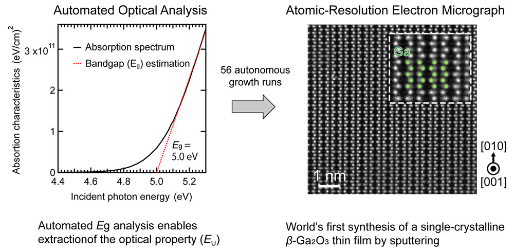 Figure 3. Realization of a single-crystalline β-Ga₂O₃ thin film by sputtering
2. Extraction of growth rules and validation through re-optimization
NTT analyzed the growth-condition and thin-film-quality data obtained during autonomous optimization using a random forest. The analysis revealed that most of the seemingly complex changes in thin-film quality could be predicted by adding together the individual effects of temperature, RF sputtering power, Ar flow rate, and O₂ flow rate.
On the other hand, the combination of temperature and O₂ flow rate could not be fully predicted through simple additive effects alone, revealing that this parameter combination requires particular attention when optimizing the growth conditions.
Based on these findings, the complex predictions learned by the random forest were distilled into a simple and readily interpretable form consisting of the contributions of the individual parameters and the interaction between temperature and O₂ flow rate (Figure 4, left).
From these insights, NTT extracted a human-executable growth rule*10: "adjust each parameter sequentially, then focus on optimizing temperature and O₂ flow rate." A researcher then performed re-optimization based on this growth rule.
As a result, the EU was further reduced to 163 meV, achieving conditions for higher-quality thin-film growth (Figure 4, right). This demonstrated that the extracted growth rule was not merely an explanation of correlations, but a practical guideline that can be used to optimize actual thin-film growth conditions.
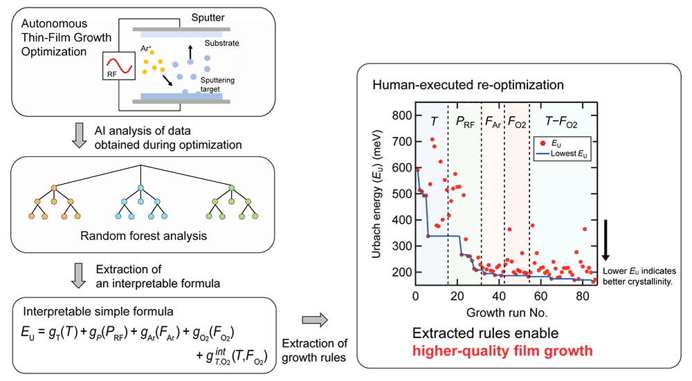 Figure 4. Extraction of growth rules and validation through re-optimization
Future Development
This technology provides a foundation for a next-generation AI-driven lab that efficiently explores multidimensional thin-film growth parameter spaces by integrating high-throughput experiments conducted by robots with machine learning for proposing growth conditions and analyzing experimental data, and connects the results to growth rules that can be understood and applied by researchers. The technology is expected to be applicable to materials and device processes involving complex condition spaces, including semiconductor materials, oxide materials, and quantum materials.
Going forward, NTT will advance optimization technologies capable of handling multiple evaluation metrics simultaneously, as well as develop more sophisticated AI models that incorporate knowledge of material properties and thin-film growth processes. NTT will also promote the automation and intelligent enhancement of experimental processes through validation using a diverse range of materials and equipment, thereby accelerating improvements in the efficiency of materials and device research.
In addition, as experimental data accumulate, NTT will further enhance and automate the proposal of growth conditions and the acquisition of scientific knowledge, developing the technology into a research platform for AI-driven labs that can conduct experiments more intelligently.
Publication Information
"Interpretable self-driving sputtering epitaxy reveals human-usable growth rules for β-Ga₂O₃ films"
Yuki K. Wakabayashi, Yui Ogawa, Franz Benedict Romero, Coleman Wagner, Takuma Otsuka, and Yoshitaka Taniyasu
Nature Communications (2026): https://doi.org/10.1038/s41467-026-76533-0
Related Past Press Releases
- October 9, 2020, "First observation of quantum transport phenomena peculiar to an exotic state"
https://group.ntt/en/newsrelease/2020/10/09/201009a.html - May 2, 2025, NTT Press release
https://group.ntt/jp/newsrelease/2025/05/02/250502a.html (Japanese)
[Glossary]
*1Self-driving thin-film growth: An experimental method that autonomously explores and improves thin-film growth conditions by combining AI-based decision-making with robotic manipulation. In this experiment, wafer transfer within the sputtering system, thin-film growth based on conditions proposed by AI, automated analysis of optical measurement data, and determination of the conditions for the next growth run were integrated into a self-driving workflow. In the current configuration, some human intervention is still required to load wafers into the load lock and to transfer samples after growth to the optical measurement system.
*2β-Ga₂O₃: A semiconductor material with a large bandgap of approximately 5 eV. A bandgap is the amount of energy required for an electron to transition to a state in which it can contribute to electrical conduction. Materials with large bandgaps can withstand high voltages and respond to short-wavelength ultraviolet light, making them promising for next-generation power devices and deep-ultraviolet optical devices.
*3Sputtering: A thin-film growth method in which a gas such as argon is converted into a plasma under vacuum, and ions in the plasma are accelerated toward and collide with a solid source material. Atoms or molecules ejected from the source material are then deposited onto a substrate. Sputtering is suitable for large-area fabrication and low-cost manufacturing and is widely used in the production of semiconductors, displays, and optical films.
*4AI for Science: An approach to advancing and accelerating scientific research using AI. It is attracting attention as a field of research that can significantly advance areas such as materials discovery, drug discovery, understanding of physical phenomena, and optimization of experimental conditions by analyzing large volumes of experimental and computational data.
*5Bayesian optimization: A machine learning method used to efficiently search for optimal conditions when the amount of observational data obtained through experiments is limited and the relationship between experimental conditions and evaluation metrics is unknown. A prediction model is constructed based on previous experimental results, and promising conditions for the next experiment are explored while taking uncertainty in the predictions into account. In this study, Bayesian optimization was used to search for conditions that improve thin-film quality across four growth parameters: temperature, RF sputtering power, Ar flow rate, and O₂ flow rate.
*6Random forest: An ensemble machine learning method that combines multiple predictive models called "decision trees." In this study, a random forest model was constructed to predict thin-film quality from growth conditions and was used to investigate which conditions have a stronger influence on thin-film quality and how combinations of conditions affect the outcome.
*7Urbach energy: An indicator derived from the optical absorption spectrum of a semiconductor or insulator that reflects the degree of optical inhomogeneity associated with defects and disorder in the material. In general, a smaller Urbach energy indicates fewer defects and less disorder, and therefore higher optical quality.
*8Heteroepitaxial growth: The growth of a crystal on a substrate made of a different material while maintaining a specific crystallographic orientation relationship between the substrate and the grown crystal.
*9Single-crystalline thin film: A thin film with a crystalline structure in which atoms are arranged in an orderly manner throughout the material. Compared with polycrystalline thin films, in which crystal orientations are not aligned, and amorphous thin films, in which the atomic arrangement is disordered, single-crystalline thin films offer greater control over electronic, optical, and thermal properties and are suitable for high-performance device applications.
*10Growth rule: A guideline for adjusting growth conditions that is extracted from the relationship between growth conditions and thin-film quality and can be understood and implemented by researchers. In this study, the extracted growth rule involves adjusting each growth parameter sequentially and then focusing on temperature and O₂ flow rate.
About NTT
NTT is a leading global technology innovator, providing a broad range of services to both consumers and businesses. As a mobile operator and provider of infrastructure, networks, and services, NTT is dedicated to promoting a sustainable future through cutting-edge innovations. Our portfolio includes business consulting, AI-powered solutions, application services, global networks, cybersecurity, data center and edge computing, all supported by our deep global industry expertise. Generating over $90 billion in revenue and employing 340,000 professionals, we allocate 30% of our annual profits to fundamental research and development. With operations spanning more than 70 countries and regions, our clients include over 75% of Fortune Global 100 companies, alongside thousands of enterprises, government organizations, and millions of consumers.
Media Contact
NTT, Inc.
NTT Science and Core Technology Laboratory Group
Public Relations
Inquiry Form
Information is current as of the date of issue of the individual press release.
Please be advised that information may be outdated after that point.


NTT STORY
WEB media that thinks about the future with NTT